9789443203
nxfee.innovation@gmail.com
Facebook Youtube Linkedin
  • VLSI PHD Research
  • *** Buy VLSI Research Projects ***
  • Freelance
  • Contact
  • VLSI Mini Projects
  • Internship
  • Archives
  • NXFEE Youtube Channel
What are you looking for?
Trending Searches: Low Power VLSI High Speed VLSI Signal Processing Image Processing
Popular categories
2014

2014

11 products
2015

2015

39 products
2016

2016

30 products
2017

2017

16 products
2018

2018

17 products
2019

2019

42 products
View all categories
My Account

Lost password?

0 0
0 Shopping Cart

No products in the cart.

Return To Shop
Shopping cart (0)
Subtotal: ₹0.00

Checkout

REFER YOUR FRIENDS WHO WILL NEED VLSI PROJECTS
“EARN Rs.1,000/- FOR ONE VLSI PROJECT” ( Amount will given After Registration )
Menu Categories
  • VLSI PHD Research
  • *** Buy VLSI Research Projects ***
  • Freelance
  • Contact
  • VLSI Mini Projects
  • Internship
  • Archives
  • NXFEE Youtube Channel
  • VLSI Application / Interface and Mini Projects
  • VLSI
  • VLSI 2024
  • NOC VLSI Design
  • VLSI 2025
  • 2017
  • VLSI 2026
  • 2014
  • 2018
  • Area Efficient
  • 2019
  • 2015
  • 2020
  • Low power VLSI Design
  • 2021
  • Image Processing
  • 2022
  • 2016
  • VLSI 2023
  • High speed VLSI Design
  • VLSI_2023
  • Accessories
  • IEEE
Cart 0
0 0
0 Shopping Cart

No products in the cart.

Return To Shop
Shopping cart (0)
Subtotal: ₹0.00

Checkout

REFER YOUR FRIENDS WHO WILL NEED VLSI PROJECTS
“EARN Rs.1,000/- FOR ONE VLSI PROJECT” ( Amount will given After Registration )
Home Shop

VLSI 2026

Return to previous page

IEEE Transactions on VLSI 2026

Following Novelty based Research Projects not yet Published in Any Journal 

Customisation Available for Journal Publications
Grid
List
Show
sale OFFER 38%
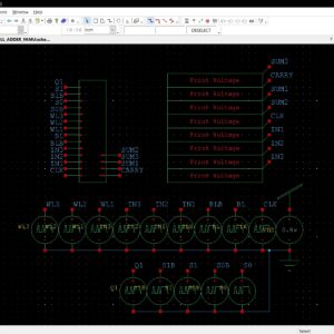
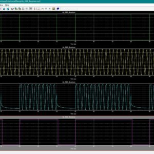
4-ASK Receiver Front-End
Quick View Add to cart
Accessories, Low power VLSI Design, VLSI, VLSI 2026

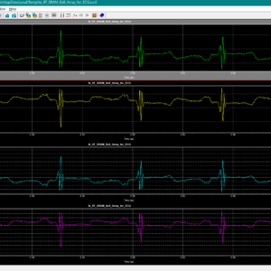
A 25-Mb/s 4-ASK Receiver Front-End in 65-nm CMOS for Biomedical Data Telemetry via a Capacitive Link

₹16,000.00 Original price was: ₹16,000.00.₹10,000.00Current price is: ₹10,000.00.
Source : Tanner EDA From : IEEE Transaction on Circuit and System II : Express Brief : Vol. 73, No. 1, January 2026. Base paper abstract:

This brief presents a 25-Mbps 4-amplitude-shiftkeying (4-ASK) receiver front-end (RFE) for biomedical data telemetry via a series-resonant capacitive link. The RFE incorporates low-power clock and data recovery (CDR) circuitry for synchronization in which a novel highly linear trans conductance (Gm) cell is employed in the phase detector (PD) to mitigate any possible error decisions while comparing the phase difference between the input and feedback signals. The proposed RFE is fabricated in 65 nm 1P8M standard CMOS, the core circuit occupies 0.11 mm2, and consumes 2.9 mA from 1 V. While conducting ex vivo measurements using beef tissue and a series-resonant capacitive link, the proposed RFE is capable of processing 4-ASK data patterns up to 25 Mbps with bit error rate (BER) less than 10−3 and total jitter of ∼42 ns. Index Terms Amplitude-shift-keying (ASK), capacitive wireless data transfer (C–WDT), clock and data recovery (CDR), receiver front-end (RFE), series-resonant capacitive link.

List of the following  materials will be included with the Downloaded Backup:
1. Source code ( Modelsim/ Xilinx/ Quartus/ DSCH3/ Microwind)
2. Existing and Proposed Project Comparison with output video 
3. Basic Documentation (20 to 30 Pages):
3.1 Proposed Title
3.2 Proposed Abstract
3.3 Advantages & Disadvantages
3.4 Improvement of this Project
3.5 Existing System with Notes
3.6 Proposed System with Notes
3.7 Literature Survey
3.8 Software Related Notes
3.9 VLSI and HDL Language / Tanner Notes
3.10 References & Reference Paper for More Pages
4. Online Support ( Any Desk / Zoom / Google Meet)
 
sale OFFER 38%
High-Precision MAC
Quick View Add to cart
Accessories, Low power VLSI Design, VLSI, VLSI 2026

A 9T SRAM Computation-in-Memory Architecture with High-Precision MAC

₹16,000.00 Original price was: ₹16,000.00.₹10,000.00Current price is: ₹10,000.00.
Source : Tanner EDA From : IEEE Transaction on VLSI System, VOL. 34, NO. 1, JANUARY 2026. Base paper abstract:

To address the data-intensive demands of modern artificial intelligence (AI) systems, computation-in-memory(CIM) based on static random-access memory (SRAM) has emerged as a promising solution by integrating computing functionality within memory arrays. However, conventional SRAM CIM architectures face two key limitations: low output resistance in single-transistor transmission paths and voltage instability on charge-sharing bitlines. These limitations collectively degrade computational accuracy to 4–5 LSB-level integral nonlinearity (INL), restricting practical deployment. This work proposes a regulated-cascode 9T SRAM cell that enhances analog computation accuracy using a high-impedance transmission path through a cascode configuration and stabilizing the discharge amount of the bitline from a single cell via active feedback regulation. Implemented in Semiconductor Manufacturing International Corporation (SMIC) 55-nm CMOS technology, the proposed cell demonstrates 1.31 LSB INL at 400-mV bitline swing (68.4% improvement versus 4–5 LSB baselines), achieving 66.7% voltage utilization efficiency compared with the conventional 50% limit and 23.04% frequency improvement is achieved compared with the conventional architecture. It also achieves an energy efficiency of 18.47 fJ/bit and a compact area of 2.655 × 1.175 µm, while demonstrating a classification accuracy of 97.7% on the MNIST dataset. Index Terms Analog linearity enhancement, multirow readout, regulated cascode circuits, static random-access memory (SRAM)-based compute-in-memory, voltage utilization efficiency.

List of the following  materials will be included with the Downloaded Backup:
1. Source code ( Modelsim/ Xilinx/ Quartus/ DSCH3/ Microwind)
2. Existing and Proposed Project Comparison with output video 
3. Basic Documentation (20 to 30 Pages):
3.1 Proposed Title
3.2 Proposed Abstract
3.3 Advantages & Disadvantages
3.4 Improvement of this Project
3.5 Existing System with Notes
3.6 Proposed System with Notes
3.7 Literature Survey
3.8 Software Related Notes
3.9 VLSI and HDL Language / Tanner Notes
3.10 References & Reference Paper for More Pages
4. Online Support ( Any Desk / Zoom / Google Meet)
 
sale OFFER 50%
Counter Based Addition Circuit
Quick View Add to cart
Accessories, Area Efficient, VLSI, VLSI 2026

A Counter Based Addition Circuit Design for Stochastic Computing

₹12,000.00 Original price was: ₹12,000.00.₹6,000.00Current price is: ₹6,000.00.
Source : Verilog HDL Base paper abstract:

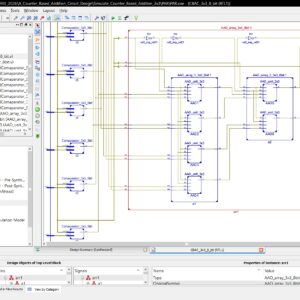
Stochastic computing (SC) encodes real values via probabilistic bitstreams, enabling complex arithmetic operations to be realized by simple logic gates. However, the requirement of longer bitstreams to ensure computing accuracy leads to higher latency, partially offsetting the low-complexity advantage of SC. To address this, this work utilizes a dynamic truncation method for stochastic bitstreams, and designs an energy-efficient counterbased addition circuit (CBAC) through effective bit recognition and correlation. Further, a tree-structured cascading architecture is then used to perform multi-input addition computing. Experimental results demonstrate that the proposed CBAC outperforms the state-of-the-art designs. For instance, a 16-input configuration achieves at least 75.9% reduction in mean square error (MSE) and a more than 43.1% reduction in area. When applied to polynomial computation and Gaussian filtering, the proposed architecture exhibits superior accuracy and efficiency, delivering MSE reductions of at least 10.7% and area reductions exceeding 6.8%.

List of the following  materials will be included with the Downloaded Backup:
1. Source code ( Modelsim/ Xilinx/ Quartus/ DSCH3/ Microwind)
2. Existing and Proposed Project Comparison with output video 
3. Basic Documentation (20 to 30 Pages):
3.1 Proposed Title
3.2 Proposed Abstract
3.3 Advantages & Disadvantages
3.4 Improvement of this Project
3.5 Existing System with Notes
3.6 Proposed System with Notes
3.7 Literature Survey
3.8 Software Related Notes
3.9 VLSI and HDL Language / Tanner Notes
3.10 References & Reference Paper for More Pages
4. Online Support ( Any Desk / Zoom / Google Meet)
 
sale OFFER 50%
Ternary
Quick View Add to cart
Accessories, Low power VLSI Design, VLSI, VLSI 2026

A T8T-SRAM Computing-in-Memory Macro for Ternary Deep Neural Networks and Boolean Logic Computations

₹12,000.00 Original price was: ₹12,000.00.₹6,000.00Current price is: ₹6,000.00.
Source : Tanner EDA Base paper abstract:

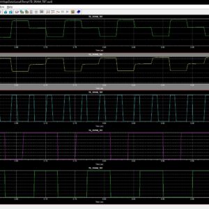
Deep neural networks (DNNs) play important roles in artificial intelligence applications and show hungry computility and power demands. Compared with binary neural networks (BNNs), ternary neural networks (TNNs) have higher representation and adaptive abilities and balance the inference accuracy and computing efficiency between DNNs and BNNs. This article proposed a T8T-SRAM computing-in-memory (CIM) macro to achieve Boolean logic operations and MAC operation of ternary activation and ternary weight. The proposed T8T-SRAM bitcell has a separate read and write path, and can avoid the read disturb issue. In Boolean logic operation mode, the T8T-SRAM macro can achieve NAND, NOR, XNOR, and XOR operations with redundant rows, reducing the additional reference voltage generation circuit. In the MAC mode, the result is quantized by an embedded column analog-to-digital converter (ADC), which uses activation refresh to reduce weight changing. In 28-nm CMOS technology, under 0.5-V array supply voltage and 0.9-V peripheral supply voltage, simulation results manifest that the MAC results have good linearity, and feasibility of Boolean logic operation. The proposed T8T-SRAM macro realizes MAC operation of 16 ternary activations and 16 ternary weights with 333.99–816.1-TOPS/W energy efficiency and 61.9-TOPS/mm2 area efficiency. Using an ResNet-18 network for the inference of MNIST, and CIFAR-10 datasets, the accuracies were 99.06% and 85.76% with a ternary activation and ternary weight.

List of the following  materials will be included with the Downloaded Backup:
1. Source code ( Modelsim/ Xilinx/ Quartus/ DSCH3/ Microwind)
2. Existing and Proposed Project Comparison with output video 
3. Basic Documentation (20 to 30 Pages):
3.1 Proposed Title
3.2 Proposed Abstract
3.3 Advantages & Disadvantages
3.4 Improvement of this Project
3.5 Existing System with Notes
3.6 Proposed System with Notes
3.7 Literature Survey
3.8 Software Related Notes
3.9 VLSI and HDL Language / Tanner Notes
3.10 References & Reference Paper for More Pages
4. Online Support ( Any Desk / Zoom / Google Meet)
 
sale OFFER 50%
Two-Stage LNA
Quick View Add to cart
Accessories, Low power VLSI Design, VLSI, VLSI 2026

A Tri-Band Two-Stage LNA with Simultaneous Linearity and Gain Enhancement for WiFi

₹12,000.00 Original price was: ₹12,000.00.₹6,000.00Current price is: ₹6,000.00.
Source : Tanner EDA Base paper abstract:

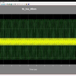
This brief presents a tri-band, two-stage compact low-noise amplifier (LNA) that simultaneously enhances linearity, gain, and noise performance for WiFi applications. The second stage adopts a dual-path architecture, consisting of a main amplifier and an additional amplifier. The additional amplifier, biased in the subthreshold region, suppresses third-order nonlinearity and enhances gain without increasing power consumption. The first-stage LNA reduces the noise contribution from the second stage, improving overall noise performance. To further minimize power consumption, an inverter-based topology is employed. Fabricated in a 90-nm CMOS process, the proposed LNA achieves an S11 below −5 dB at 2.4, 5, and 6 GHz, covering key WiFi bands. At 6-GHz band, it delivers 13.5-dB gain, 3.2-dBm third-order input intercept point (IIP3), and 3.1-dB noise figure (NF). At 5-GHz band, it achieves 15-dB gain, 0.7-dBm IIP3, and 2.76-dB NF. At 2.4-GHz band, it provides 20.66-dB gain, −7-dBm IIP3, and 2.7-dB NF. The circuit consumes only 3 mW of dc power. Measurements at 6 GHz show that the dual-path technique in the second stage improves IIP3 by 8.6 dB, increases gain by 1.5 dB, and reduces NF by 0.6 dB, all without additional power or area overhead.

List of the following  materials will be included with the Downloaded Backup:
1. Source code ( Modelsim/ Xilinx/ Quartus/ DSCH3/ Microwind)
2. Existing and Proposed Project Comparison with output video 
3. Basic Documentation (20 to 30 Pages):
3.1 Proposed Title
3.2 Proposed Abstract
3.3 Advantages & Disadvantages
3.4 Improvement of this Project
3.5 Existing System with Notes
3.6 Proposed System with Notes
3.7 Literature Survey
3.8 Software Related Notes
3.9 VLSI and HDL Language / Tanner Notes
3.10 References & Reference Paper for More Pages
4. Online Support ( Any Desk / Zoom / Google Meet)
 
sale OFFER 50%
CIM_Macro
Quick View Add to cart
Accessories, Low power VLSI Design, VLSI, VLSI 2026

An Approximate Digital CIM Macro with Low-Power Multiply-Add Units

₹12,000.00 Original price was: ₹12,000.00.₹6,000.00Current price is: ₹6,000.00.
Source : Tanner EDA Base paper abstract:

This letter presents an approximate digital compute-in memory (CIM) macro for low-power edge AI inference. It introduces three hierarchical innovations: 1) novel fused approximate multiply-add units (FAMUs) that reduces power and area consumption; 2) a bit-critical weight allocation architecture that optimally balances accuracy and hardware cost; and 3) a dynamic sparsity-adaptive configuration method to minimize accuracy loss in real-time. The macro achieves an energy efficiency of 60.35 TOPS/W and an area efficiency of 1105 GOPS/mm2 for INT8 MACs, outperforming prior works. It attains negligible accuracy degradation on multiple mainstream datasets and suits well for edge AI inference.

List of the following  materials will be included with the Downloaded Backup:
1. Source code ( Modelsim/ Xilinx/ Quartus/ DSCH3/ Microwind)
2. Existing and Proposed Project Comparison with output video 
3. Basic Documentation (20 to 30 Pages):
3.1 Proposed Title
3.2 Proposed Abstract
3.3 Advantages & Disadvantages
3.4 Improvement of this Project
3.5 Existing System with Notes
3.6 Proposed System with Notes
3.7 Literature Survey
3.8 Software Related Notes
3.9 VLSI and HDL Language / Tanner Notes
3.10 References & Reference Paper for More Pages
4. Online Support ( Any Desk / Zoom / Google Meet)
 
sale OFFER 50%
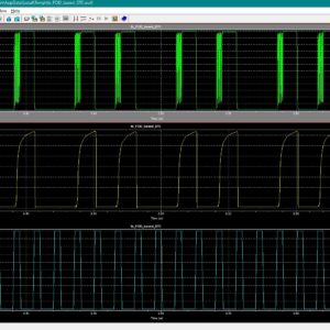
Fractional Output Divider
Quick View Add to cart
Accessories, Low power VLSI Design, VLSI, VLSI 2026

An Area-Efficient Fractional Output Divider Based on Foreground DTC INL Calibration

₹12,000.00 Original price was: ₹12,000.00.₹6,000.00Current price is: ₹6,000.00.
Source : Tanner EDA From : IEEE Transaction on VLSI System, VOL. 73, NO. 1, JANUARY 2026. Base paper abstract:

This brief presents a fractional output divider (FOD) with a foreground digital-to-time converter (DTC) INL calibration scheme. This calibration scheme adjusts the delay control words of two main DTCs (mDTCs) to enable mutual comparison between them. By using a sign-least-mean-squares (sign-LMS) algorithm, the INL error codes are obtained and subsequently applied to a calibration DTC (cDTC) to compensate for the mDTC INL. The prototype occupies a compact core area of 0.01mm2 and operates at a 0.9V supply with a power consumption of 3.6mW at 500MHz. Measurements demonstrate an integrated jitter of 512fs (10kHz to 20MHz) and spur level of -70dBc at 123.46MHz. Index Terms—Fractional output divider (FOD), frequency synthesis, digital-to-time converter (DTC), integral nonlinearity (INL), foreground calibration, bang-bang phase detector (BBPD).

List of the following  materials will be included with the Downloaded Backup:
1. Source code ( Modelsim/ Xilinx/ Quartus/ DSCH3/ Microwind)
2. Existing and Proposed Project Comparison with output video 
3. Basic Documentation (20 to 30 Pages):
3.1 Proposed Title
3.2 Proposed Abstract
3.3 Advantages & Disadvantages
3.4 Improvement of this Project
3.5 Existing System with Notes
3.6 Proposed System with Notes
3.7 Literature Survey
3.8 Software Related Notes
3.9 VLSI and HDL Language / Tanner Notes
3.10 References & Reference Paper for More Pages
4. Online Support ( Any Desk / Zoom / Google Meet)
 
sale OFFER 33%
Internal Self-Healing
Quick View Add to cart
Accessories, Area Efficient, VLSI, VLSI 2026

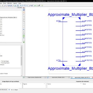
Approximate Multiplier for Power Efficiency in FPGA Design Using Internal Self-Healing

₹12,000.00 Original price was: ₹12,000.00.₹8,000.00Current price is: ₹8,000.00.
Source : Verilog HDL Base paper abstract:

Approximate Computing has emerged as a viable solution to resource constraints in computing for error-resilient applications by relaxing accuracy for significant gains in terms of power, performance, and area. Among existing approximation techniques, the self-healing methodologies have shown a promising quality-efficiency balance by canceling out the overall effect of computational errors. However, they rely on highly parallel implementations for error cancellation. In our prior work (MACISH), we proposed an Internal-Self-Healing (ISH) methodology that applies approximations in the recursive multiplication stage and leverages the accumulation stage for error cancellation, eliminating the need for paired parallel modules required by traditional self-healing approaches. ASIC-based digital designs proposed by MACISH demonstrated superior quality-efficiency results for the radio astronomy application. However, the architectural differences limit the direct mapping of ASIC-based optimized designs to FPGAs. Therefore, this article addresses the gap by designing the FPGA-based Pareto-optimal 4-bit and 8-bit recursive approximate multipliers using ISH methodology. The proposed Design Space Exploration (DSE) strategy manages the vast 8-bit design space by deriving the candidate designs from 4-bit Pareto-optimal multipliers, reducing the search complexity while preserving the performance. The proposed designs achieve up to 12% and 33.6% better power and energy efficiency, respectively, compared to accurate 8-bit multipliers and up to 30× improved output quality at a similar area. The design flow is automated using the ‘Approxy’ Tool, which has also been developed as part of this work. For the radio astronomy correlation application, these designs achieved comparable (and acceptable) output quality with respect to the state-of-the-art. For Deep Learning (DL) workloads, the proposed 8-bit designs matched or even exceeded the baseline accuracy for binary and multiclass classification problems.

List of the following  materials will be included with the Downloaded Backup:
1. Source code ( Modelsim/ Xilinx/ Quartus/ DSCH3/ Microwind)
2. Existing and Proposed Project Comparison with output video 
3. Basic Documentation (20 to 30 Pages):
3.1 Proposed Title
3.2 Proposed Abstract
3.3 Advantages & Disadvantages
3.4 Improvement of this Project
3.5 Existing System with Notes
3.6 Proposed System with Notes
3.7 Literature Survey
3.8 Software Related Notes
3.9 VLSI and HDL Language / Tanner Notes
3.10 References & Reference Paper for More Pages
4. Online Support ( Any Desk / Zoom / Google Meet)
 
sale OFFER 44%
Systolic Array for Matrix Multiplication
Quick View Add to cart
Accessories, Area Efficient, VLSI, VLSI 2026

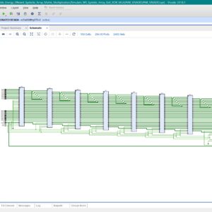
DiP: A Scalable, Energy-Efficient Systolic Array for Matrix Multiplication Acceleration

₹18,000.00 Original price was: ₹18,000.00.₹10,000.00Current price is: ₹10,000.00.
Source : Verilog HDL Base paper abstract:

Transformers are gaining increasing attention across Natural Language Processing (NLP) application domains due to their outstanding accuracy. However, these data-intensive models add significant performance demands to the existing computing architectures. Systolic array architectures, adopted by commercial AI computing platforms like Google TPUs, offer energy-efficient data reuse but face throughput and energy penalties due to input-output synchronization via First-In-FirstOut (FIFO) buffers. This paper proposes a novel scalable systolic array architecture featuring Diagonal-Input and Permutated weight stationary (DiP) dataflow for matrix multiplication acceleration. The proposed architecture eliminates the synchronization FIFOs required by state-of-the-art weight stationary systolic arrays. Beyond the area, power, and energy savings achieved by eliminating these FIFOs, DiP architecture maximizes the computational resource utilization, achieving up to 50% throughput improvement over conventional weight stationary architectures. Analytical models are developed for both weight stationary and DiP architectures, including latency, throughput, time to full PEs utilization (TFPU), and FIFOs overhead. A comprehensive hardware design space exploration using 22nm commercial technology demonstrates DiP’s scalability advantages, achieving up to a 2.02× improvement in energy efficiency per area. Furthermore, DiP outperforms TPU-like architectures on transformer workloads from widely-used models, delivering energy improvement up to 1.81× and latency improvement up to 1.49×. At a 64×64 size with 4096 PEs, DiP achieves a peak throughput of 8.192 TOPS with energy efficiency 9.548 TOPS/W.

List of the following  materials will be included with the Downloaded Backup:
1. Source code ( Modelsim/ Xilinx/ Quartus/ DSCH3/ Microwind)
2. Existing and Proposed Project Comparison with output video 
3. Basic Documentation (20 to 30 Pages):
3.1 Proposed Title
3.2 Proposed Abstract
3.3 Advantages & Disadvantages
3.4 Improvement of this Project
3.5 Existing System with Notes
3.6 Proposed System with Notes
3.7 Literature Survey
3.8 Software Related Notes
3.9 VLSI and HDL Language / Tanner Notes
3.10 References & Reference Paper for More Pages
4. Online Support ( Any Desk / Zoom / Google Meet)
 
IEEE Transactions on VLSI 2026, VLSI 2026 IEEE Project, VLSI Low Power 2026 Project, VLSI High Speed 2026 Project, VLSI Area Efficient 2026 Project, Low-Cost VLSI 2026 Projects, High-Speed VLSI Design 2026 projects (CDMA, RTOS, DSP, RF, IF, etc.), Low Power VLSI Design 2026 projects, Area Efficient VLSI Design 2026 projects, Audio processing VLSI Design 2026 projects, Signal Processing VLSI Design 2026 projects, Image Processing VLSI Design 2026 projects, Backend VLSI Design 2026 projects (CMOS, TFET, BisFET, FeFET, etc.), Timing & Delay Reduction VLSI 2026 Projects, Internet of Things VLSI 2026 Projects, Testing, Reliability and Fault Tolerance VLSI Projects, VLSI Applications (Communicational, Video, Security, Sensor Networks, etc.), SOC VLSI Projects, Network on Chip VLSI Projects, Wireless Communication VLSI Projects, VLSI Verifications Projects (UVM, OVM, VVM, System Verilog).

Provide Wordlwide Online Support

We can provide Online Support Wordlwide, with proper execution, explanation and additionally provide explanation video file for execution and explanations.

24/7 Support Center

NXFEE, will Provide on 24x7 Online Support, You can call or text at +91 9789443203, or email us nxfee.innovation@gmail.com

Terms & Conditions:

Customer are advice to watch the project video file output, and before the payment to test the requirement, correction will be applicable.

After payment, if any correction in the Project is accepted, but requirement changes is applicable with updated charges based upon the requirement.

After payment the student having doubts, correction, software error, hardware errors, coding doubts are accepted.

Online support will not be given more than 3 times.

On first time explanation we can provide completely with video file support, other 2 we can provide doubt clarifications only.

If any Issue on Software license / System Error we can support and rectify that within end of day.

Extra Charges For duplicate bill copy. Bill must be paid in full, No part payment will be accepted.

After payment, to must send the payment receipt to our email id.

Powered by NXFEE INNOVATION, Pondicherry.

Call us today at : +91 9789443203 or Email us at nxfee.innovation@gmail.com

Contact us

NXFEE Development & Services

NXFEE Software Projects

Product Categories

  • 2014 (11)
  • 2015 (39)
  • 2016 (30)
  • 2017 (16)
  • 2018 (17)
  • 2019 (42)
  • 2020 (29)
  • 2021 (17)
  • 2022 (23)
  • Accessories (54)
  • Area Efficient (119)
  • High speed VLSI Design (59)
  • IEEE (15)
  • Image Processing (40)
  • Low power VLSI Design (102)
  • NOC VLSI Design (2)
  • VLSI (260)
  • VLSI 2023 (21)
  • VLSI 2024 (18)
  • VLSI 2025 (33)
  • VLSI 2026 (9)
  • VLSI Application / Interface and Mini Projects (33)
  • VLSI_2023 (15)

Filter by price

Price: —

Product Status

  • In stock
  • Out of stock
  • On sale

Sort by producents

    Refer and Earn

    THANK YOU

    Thank for Visit NXFEE Innovation, Get in touch with Best Semiconductor IP Development. 

    Our services

    • Company Information
    • Terms and Conditions for Sales
    • Privacy policy
    • Returns and refunds

    Quick Links

    • VLSI PHD Research
    • About NXFEE
    • Contact NXFEE

    Contact us :

    • 45, First Floor, Vivekanandar Street, Dhevan Kandappa Mudaliar Nagar, Nainarmandapam, Pondicherry - 605004. India.
    • nxfee.innovation@gmail.com
    • +91 9789443203, 0413-2968203.

    Our services

    • Company Information
    • Terms and Conditions for Sales
    • Privacy policy
    • Returns and refunds

    Quick Links

    • VLSI PHD Research
    • About NXFEE
    • Contact NXFEE

    Contact us :

    • 45, First Floor, Vivekanandar Street, Dhevan Kandappa Mudaliar Nagar, Nainarmandapam, Pondicherry - 605004. India.
    • nxfee.innovation@gmail.com
    • +91 9789443203, 0413-2968203.
    Facebook Twitter Whatsapp Email Youtube

    Copyright © 2026 Nxfee Innovation.

    Home
    Shop
    0 Cart
    More
    More
    • VLSI PHD Research
    • *** Buy VLSI Research Projects ***
    • Freelance
    • Contact
    • VLSI Mini Projects
    • Internship
    • Archives
    • NXFEE Youtube Channel

    WhatsApp