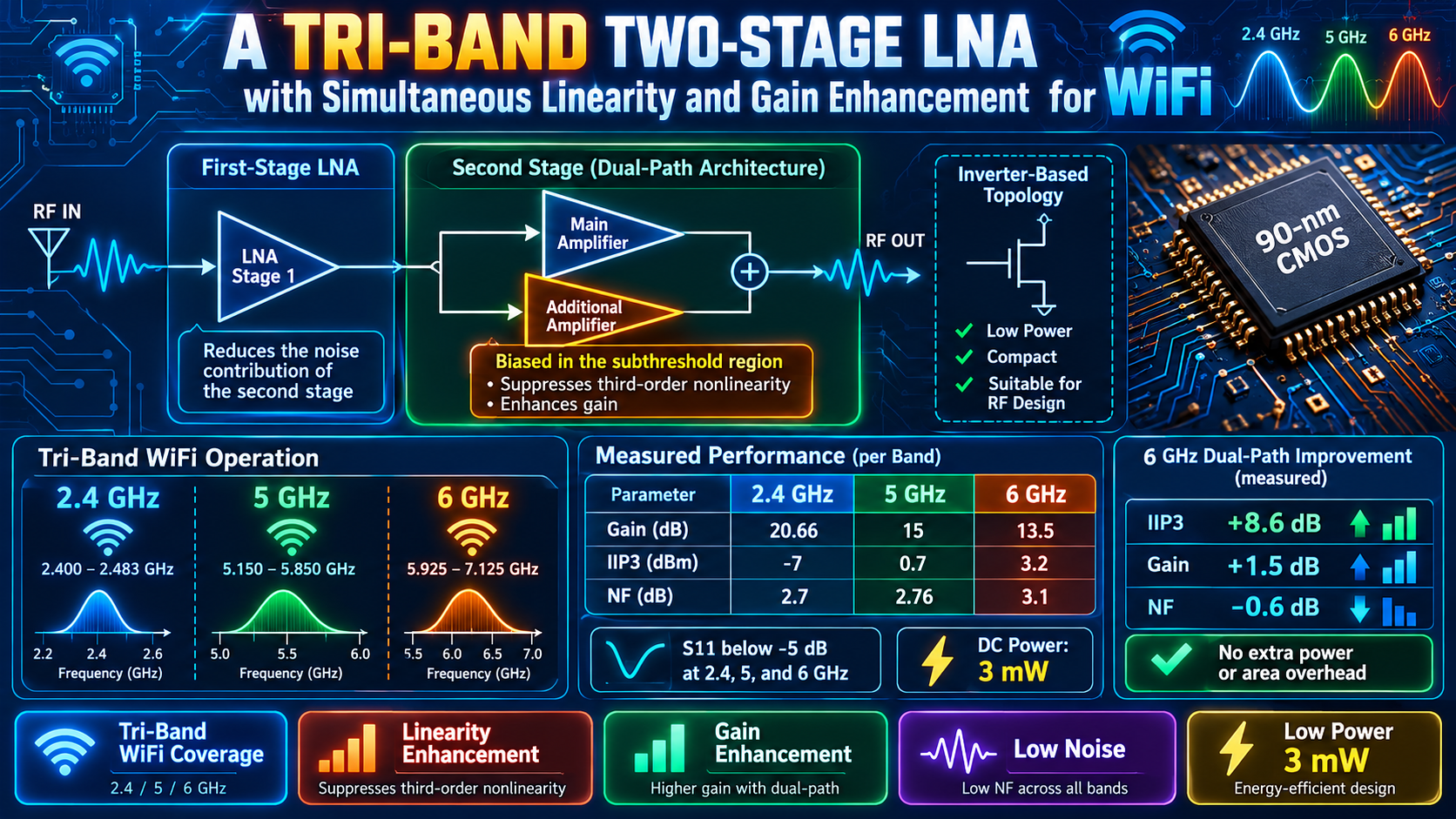
Improvement of this project:
- To design the proposed work and validated the LNA under two different excitation methods, sinusoidal and PWM, and providing a comprehensive performance evaluation.
- To design this work in 45nm CMOS Technology and significantly reduces power consumption and compared with the 90nm design, while maintaining comparable voltage gain
Proposed abstract:
Low-noise amplifiers (LNAs) are one of the most important building blocks in wireless communication systems, Internet of Things (IoT) devices, WiFi transceivers, sensor networks, and portable RF applications because they amplify weak received signals while maintaining low distortion and low power consumption. Although conventional LNA architectures provide high gain and good RF performance, they often suffer from high power consumption, larger silicon area, and increased implementation complexity, especially when advanced RF techniques are incorporated. Several existing works have focused on improving gain, linearity, and noise performance; however, many of these designs are implemented using older CMOS technologies and primarily evaluate RF characteristics without investigating the effect of different input excitation methods on circuit performance. To address these limitations, this work presents a power-efficient two-stage low-noise amplifier implemented using 45 nm CMOS technology and verified in the Tanner EDA design environment. The proposed design evaluates the amplifier under both sinusoidal and pulse-width modulation (PWM) input excitations to investigate their influence on power consumption, propagation delay, and voltage gain. The novelty of this work lies in performing a comparative analysis of two different input excitation techniques on the same LNA architecture, demonstrating that PWM excitation significantly reduces power consumption while maintaining comparable voltage gain and stable operating characteristics. Simulation results show that the proposed LNA occupies an area of 1.093 µm² with six MOSFETs and operates from a 0.6 V supply. The design achieves an estimated voltage gain of approximately 15.56 dB, an average power consumption of 944.82 µW under sinusoidal excitation and 422.74 µW under PWM excitation, representing nearly 55% power reduction, with propagation delays of 1.6045 µs and 1.6195 µs, respectively. These results confirm that the proposed implementation provides an energy-efficient and compact solution suitable for future low-power RF integrated circuit applications.
” Thanks for Visit this project Pages – Buy It Soon “
Design and Performance Analysis of a 45nm CMOS Two Stage Low Noise Amplifier under Sinusoidal and PWM Excitation.
Terms & Conditions:
- Customer are advice to watch the project video file output, before the payment to test the requirement, correction will be applicable.
- After payment, if any correction in the Project is accepted, but requirement changes is applicable with updated charges based upon the requirement.
- After payment the student having doubts, correction, software error, hardware errors, coding doubts are accepted.
- Online support will not be given more than 3 times.
- On first time explanations we can provide completely with video file support, other 2 we can provide doubt clarifications only.
- If any Issue on Software license / System Error we can support and rectify that within end of the day.
- Extra Charges For duplicate bill copy. Bill must be paid in full, No part payment will be accepted.
- After payment, to must send the payment receipt to our email id.
- Powered by NXFEE INNOVATION, Pondicherry.
Payment Method :
- Pay Add to Cart Method on this Page
- Deposit Cash/Cheque on our a/c.
- Pay Google Pay/Phone Pay : +91 9789443203
- Send Cheque through courier
- Visit our office directly
- Pay using Paypal : Click here to get NXFEE-PayPal link
Bank Accounts
HDFC BANK ACCOUNT:
- NXFEE INNOVATION,
HDFC BANK, MAIN BRANCH, PONDICHERRY-605004.
INDIA,
ACC NO. 50200090465140,
IFSC CODE: HDFC0000407.