Improvement of this project:
- The proposed 22 nm T8T-SRAM architecture improves hardware compactness by reducing the silicon area compared with the existing 28 nm implementation.
- The optimized T8T-SRAM, Boolean logic, Sense Amplifier, and MAC circuits reduce average power consumption while maintaining reliable and efficient in-memory computation.
- The proposed design enhances overall VLSI performance by providing lower hardware overhead, improved integration density, and suitability for future low-power Computing-in-Memory (CIM) and AI edge applications.
Proposed abstract:
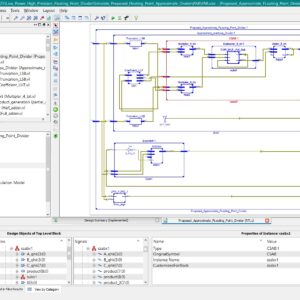
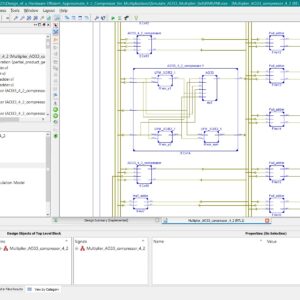
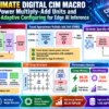
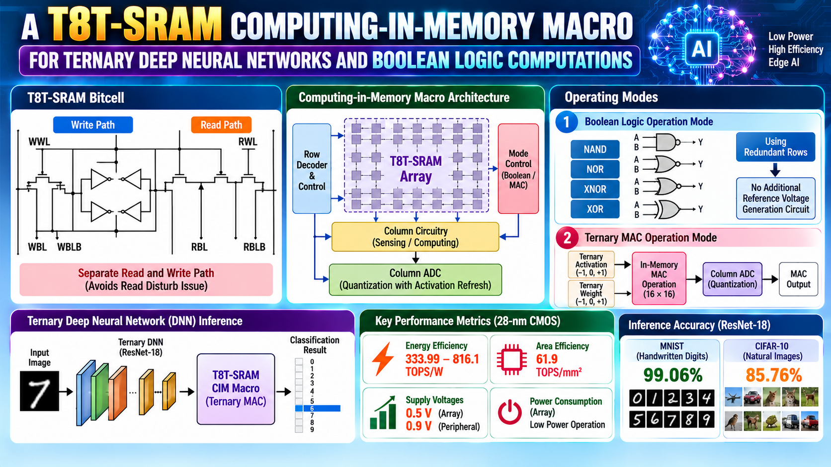
Computing-in-Memory (CIM) based SRAM architectures have emerged as a promising solution for artificial intelligence, edge computing, Internet of Things (IoT), and low-power embedded systems by reducing data movement between memory and processing units, thereby improving computational speed and energy efficiency. However, existing SRAM-CIM designs, including recently reported 28 nm implementations, still face challenges such as larger silicon area, increased transistor count, higher power consumption, longer propagation delay, and complex hardware integration for Boolean logic and multiply-and-accumulate (MAC) operations. Although the reported 28 nm T8T-SRAM architecture demonstrated improved computing capability for ternary neural networks, there is still a need for a more compact and power-efficient circuit implementation suitable for future VLSI systems. To address these limitations, this work proposes a compact T8T-SRAM based architecture implemented using 22 nm CMOS technology in the Tanner EDA environment. The proposed work includes the design and implementation of an optimized 8T-SRAM, T8T-SRAM, NAND, NOR, XOR, XNOR, Sense Amplifier (SA), and MAC circuits, forming the essential building blocks for future SRAM-CIM architectures. The novelty of the proposed work lies in implementing these optimized circuit blocks in a smaller 22 nm technology node while reducing hardware overhead and improving circuit compactness compared with the existing 28 nm implementation. The proposed design is prioritized to support future low-power and high-density in-memory computing applications with reduced silicon area and improved hardware efficiency. The circuits were designed, simulated, and verified using Tanner EDA, and their performance was evaluated in terms of layout area, transistor count, propagation delay, and average power consumption. The obtained results demonstrate that the proposed 22 nm implementation provides a compact, reliable, and energy-efficient hardware solution, making it a strong candidate for next-generation SRAM-based computing-in-memory systems and advanced VLSI applications.
” Thanks for Visit this project Pages – Buy It Soon “
Design and Implementation of a 22nm CMOS T8T-SRAM with Integrated Boolean Logic and MAC Circuit using Tanner EDA
Terms & Conditions:
- Customer are advice to watch the project video file output, before the payment to test the requirement, correction will be applicable.
- After payment, if any correction in the Project is accepted, but requirement changes is applicable with updated charges based upon the requirement.
- After payment the student having doubts, correction, software error, hardware errors, coding doubts are accepted.
- Online support will not be given more than 3 times.
- On first time explanations we can provide completely with video file support, other 2 we can provide doubt clarifications only.
- If any Issue on Software license / System Error we can support and rectify that within end of the day.
- Extra Charges For duplicate bill copy. Bill must be paid in full, No part payment will be accepted.
- After payment, to must send the payment receipt to our email id.
- Powered by NXFEE INNOVATION, Pondicherry.
Payment Method :
- Pay Add to Cart Method on this Page
- Deposit Cash/Cheque on our a/c.
- Pay Google Pay/Phone Pay : +91 9789443203
- Send Cheque through courier
- Visit our office directly
- Pay using Paypal : Click here to get NXFEE-PayPal link
Bank Accounts
HDFC BANK ACCOUNT:
- NXFEE INNOVATION,
HDFC BANK, MAIN BRANCH, PONDICHERRY-605004.
INDIA,
ACC NO. 50200090465140,
IFSC CODE: HDFC0000407.