Improvement of this project:
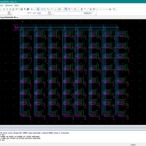
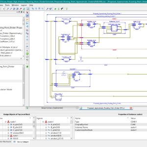
- Implement the design of FMAU1, FMAU2, FMAU3 using 45nm CMOS technology at 0.8v, and compare the work in to the paper 55nm CMOS technology and proved the performance.
- Evaluated power consumption, propagation delay, transistor count and area under identical operation conditions.
Proposed abstract:
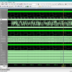
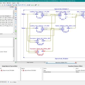
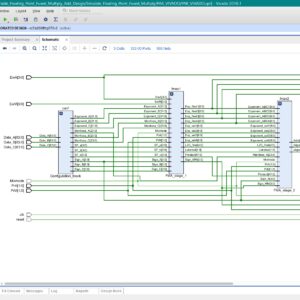
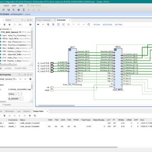
Compute-in-Memory (CIM) has become an important architecture for artificial intelligence, edge computing, Internet of Things (IoT), and embedded systems because it performs data processing within the memory array, thereby reducing data movement, execution latency, and energy consumption. Among various CIM approaches, digital approximate CIM provides better reliability than analog CIM while maintaining high computational efficiency. However, conventional digital CIM architectures require separate multiplier and adder circuits, resulting in increased hardware complexity, power consumption, and silicon area. To overcome these limitations, this work introduced a Fused Approximate Multiply-Add Unit (FAMU), which combines multiplication and addition into a single compact circuit to reduce hardware overhead. The work further proposed three FAMU variants, namely FAMU1, FAMU2, and FAMU3, where FAMU1 provides minimum hardware cost, FAMU2 offers improved approximation accuracy, and FAMU3 achieves the highest computational accuracy among the approximate units. These circuits are integrated with a bit-critical weight allocation architecture and a dynamic sparse-adaptive configuration technique to balance computational accuracy and energy efficiency for edge AI inference. In this work, the proposed FAMU1, FAMU2, and FAMU3 architectures are implemented and analyzed using 45 nm CMOS technology at a supply voltage of 0.8 V to evaluate the impact of technology scaling on the original design. The novelty of this work lies in validating the original FAMU architecture under an advanced CMOS process and demonstrating improved hardware performance without modifying its operating principle. The circuits are designed and simulated using the Tanner EDA Tool, and their performance is compared with the reported 55 nm CMOS implementation in terms of power consumption, propagation delay, transistor count, area, and energy efficiency. The obtained results demonstrate that the 45 nm implementation provides lower power dissipation, reduced delay, and improved overall efficiency while preserving the functionality and approximation characteristics of the original FAMU-based compute-in-memory architecture.
” Thanks for Visit this project Pages – Buy It Soon “
Performance Evaluation of Fused Approximate Multiply-Add-Units using 45nm CMOS Technology for Compute-in-Memory Application
Terms & Conditions:
- Customer are advice to watch the project video file output, before the payment to test the requirement, correction will be applicable.
- After payment, if any correction in the Project is accepted, but requirement changes is applicable with updated charges based upon the requirement.
- After payment the student having doubts, correction, software error, hardware errors, coding doubts are accepted.
- Online support will not be given more than 3 times.
- On first time explanations we can provide completely with video file support, other 2 we can provide doubt clarifications only.
- If any Issue on Software license / System Error we can support and rectify that within end of the day.
- Extra Charges For duplicate bill copy. Bill must be paid in full, No part payment will be accepted.
- After payment, to must send the payment receipt to our email id.
- Powered by NXFEE INNOVATION, Pondicherry.
Payment Method :
- Pay Add to Cart Method on this Page
- Deposit Cash/Cheque on our a/c.
- Pay Google Pay/Phone Pay : +91 9789443203
- Send Cheque through courier
- Visit our office directly
- Pay using Paypal : Click here to get NXFEE-PayPal link
Bank Accounts
HDFC BANK ACCOUNT:
- NXFEE INNOVATION,
HDFC BANK, MAIN BRANCH, PONDICHERRY-605004.
INDIA,
ACC NO. 50200090465140,
IFSC CODE: HDFC0000407.