HDFC BANK ACCOUNT:
- NXFEE INNOVATION,
HDFC BANK, MAIN BRANCH, PONDICHERRY-605004.
INDIA,
ACC NO. 50200090465140,
IFSC CODE: HDFC0000407.

₹35,000.00 Original price was: ₹35,000.00.₹30,000.00Current price is: ₹30,000.00.
Source : Verilog HDL
Base paper abstract:
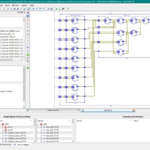
5G new radio supports a variety of new technologies and services, demanding significant improvements in radio access network (RAN) latency, throughput, and flexibility. Disaggregation addresses these challenges by splitting the RAN into network units–central (CU), distributing (DU), and radio (RU), enabling data processing virtualization and implementation on off-the-shelf hardware. However, implementing upper physical layer (PHY) processing on off-the-shelf hardware alone might cause inefficient usage of the server processors. Therefore, acceleration is often needed to offload heavy processing, focusing on low-density parity-check (LDPC) codec as the most compute-intensive task in the PHY. Additionally, LDPC coding is tightly coupled with rate-matching. This paper presents novel hardware architectures of rate-matcher and rate-dematcher, targeting field programmable gate array (FPGA) RAN accelerators. The presented solution’s approach to memory organization allows highly parallel operation with efficient hardware resource usage. The architecture is flexible, enabling a selection of various parallelism levels for instant integration with other PHY components, and achieves a throughput of up to 150 Gbps for ratematching, and up to 35 Gbps for rate-dematching. Both components have been integrated into a Peripheral Component Interconnect Express (PCIe) FPGA acceleration card with an LDPC encoder and decoder. The accelerator performance has been evaluated against OpenAirInterface PHY software. By measuring the acceleration impact on the processor load, it has been shown that with the proposed components, the acceleration efficiency can be increased by an order of magnitude compared to the LDPC-only solution.
List of the following materials will be included with the Downloaded Backup:
Objective of this work :
Proposed abstract:
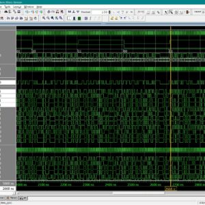
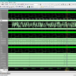
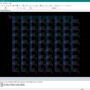
Modern wireless communication systems such as 5G, satellite communication, IoT networks, and high-speed data links require efficient modulation and high-throughput digital processing to meet increasing performance demands. QPSK modulation is widely adopted due to its simplicity, robustness, and moderate spectral efficiency, making it suitable for practical FPGA-based implementations. However, such systems face challenges including limited transmission bandwidth, mismatch between high-speed digital processing and RF constraints, and inefficient utilization of hardware resources in existing designs. Most current implementations focus either on modulation/demodulation or coding techniques, without addressing the integration of high-speed parallel data handling with efficient hardware utilization. In this work, a complete FPGA-based communication system is developed using 4-QPSK modulation and demodulation with an 8-bit parallel data path operating at a 500 MHz system clock, achieving a peak digital throughput of 4 Gbps. The design highlights the practical limitation of transmission under a 27.77 MHz carrier frequency, emphasizing the gap between processing capability and actual communication rate. The proposed architecture focuses on pipeline optimization, synchronization, and efficient data flow to improve system performance. The novelty of this work lies in demonstrating a high-speed parallel processing architecture integrated with QPSK communication while analyzing the disparity between digital throughput and bandwidth-limited transmission, providing a scalable foundation for future OFDM-based systems. The design is implemented and functionally verified using ModelSim simulation, and further synthesized on an Artix-7 FPGA to evaluate hardware performance. Resource utilization and efficiency are analyzed in terms of LUTs, flip-flops, delay, and power consumption, showing optimized hardware usage with reliable operation. The results confirm that the proposed system achieves high-speed performance with efficient resource utilization, making it suitable for advanced communication system development.
” Thanks for Visit this project Pages – Buy It Soon “
Payment Method :
HDFC BANK ACCOUNT:
₹18,000.00 Original price was: ₹18,000.00.₹10,000.00Current price is: ₹10,000.00.


₹16,000.00 Original price was: ₹16,000.00.₹12,000.00Current price is: ₹12,000.00.
Copyright © 2026 Nxfee Innovation.
Scalable 5G NR Rate Matcher an...
₹35,000.00 Original price was: ₹35,000.00.₹30,000.00Current price is: ₹30,000.00.