9789443203
nxfee.innovation@gmail.com
Facebook Youtube Linkedin
  • VLSI PHD Research
  • *** Buy VLSI Research Projects ***
  • Freelance
  • Contact
  • VLSI Mini Projects
  • Internship
  • Archives
  • NXFEE Youtube Channel
What are you looking for?
Trending Searches: Low Power VLSI High Speed VLSI Signal Processing Image Processing
Popular categories
2014

2014

11 products
2015

2015

39 products
2016

2016

30 products
2017

2017

16 products
2018

2018

17 products
2019

2019

42 products
View all categories
My Account

Lost password?

0 0
0 Shopping Cart

No products in the cart.

Return To Shop
Shopping cart (0)
Subtotal: ₹0.00

Checkout

REFER YOUR FRIENDS WHO WILL NEED VLSI PROJECTS
“EARN Rs.1,000/- FOR ONE VLSI PROJECT” ( Amount will given After Registration )
Menu Categories
  • VLSI PHD Research
  • *** Buy VLSI Research Projects ***
  • Freelance
  • Contact
  • VLSI Mini Projects
  • Internship
  • Archives
  • NXFEE Youtube Channel
  • VLSI Application / Interface and Mini Projects
  • VLSI
  • VLSI 2024
  • NOC VLSI Design
  • VLSI 2025
  • 2017
  • VLSI 2026
  • 2014
  • 2018
  • Area Efficient
  • 2019
  • 2015
  • 2020
  • Low power VLSI Design
  • 2021
  • Image Processing
  • 2022
  • 2016
  • VLSI 2023
  • High speed VLSI Design
  • VLSI_2023
  • Accessories
  • IEEE
Cart 0
0 0
0 Shopping Cart

No products in the cart.

Return To Shop
Shopping cart (0)
Subtotal: ₹0.00

Checkout

REFER YOUR FRIENDS WHO WILL NEED VLSI PROJECTS
“EARN Rs.1,000/- FOR ONE VLSI PROJECT” ( Amount will given After Registration )
Home Shop Low power VLSI Design Page 2

Page 2

Return to previous page
Grid
List
Show
sale OFFER 40%
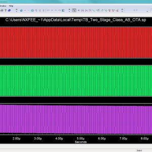
Two Stage OTA
Quick View Add to cart
2022, Low power VLSI Design, VLSI

Two-Stage OTA With All Subthreshold MOSFETs and Optimum GBW to DC-Current Ratio

₹10,000.00 Original price was: ₹10,000.00.₹6,000.00Current price is: ₹6,000.00.
Source : Tanner EDA

Base Paper Abstract:

An approach for the design of two-stage class AB OTAs with sub-1µA current consumption is proposed and demonstrated. The approach employs MOS transistors operating in subthreshold and allows maximum gain-bandwidth product (GBW) to be achieved for a given DC current budget, by setting optimum distribution of DC currents in the two amplifier stages. Following this strategy, a class AB OTA was designed in a standard 0.5-µm CMOS technology supplied from 1.6-V and experimentally tested. Measured GBW was 307 kHz with 980-nA DC current consumption while driving an output capacitance of 40 pF with an average slew rate of 96 V/ms.

List of the following  materials will be included with the Downloaded Backup:
1. Source code ( Modelsim/ Xilinx/ Quartus/ DSCH3/ Microwind)
2. Existing and Proposed Project Comparison
3. Architecture Diagram
4. Algorithm with Flow chart
5. Report for Phase1 and Phase2
6. Proposed abstract document
7. Reference materials
8. Literature survey with Reference Document
9. Online Support ( Team viewer/ Ammy Admin)
sale OFFER 50%
Vital-Sign Processing
Quick View Add to cart
2020, Low power VLSI Design, VLSI

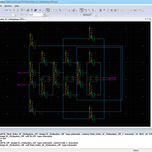
Vital-Sign Processing Receiver With Clutter Elimination Using Servo Feedback Loop for UWB Pulse Radar System

₹12,000.00 Original price was: ₹12,000.00.₹6,000.00Current price is: ₹6,000.00.
Source : Tanner EDA

Abstract:

This brief presents a vital-sign processing circuit for simultaneous dc/near-dc elimination and out-of-band interference rejection without any digital signal processing or algorithm assistance for the ultra wideband (UWB) pulse-based radar system. An intrinsic self balanced MOS diode (SBMD) was proposed as a stable and balanced pseudo resistor applied under a servo feedback loop in a vital-sign receiver of the sensing radar to perform as a high-pass filter (HPF) with an ultralow corner frequency lower than 0.5 Hz for removing undesired clutters of the reflected signals and input dc-offset voltages from innate circuit offsets. A third-order switched-capacitor (SC) Chebyshev low-pass filter (LPF) with leap-frog topology as the subsequent stage was adopted to suppress the out-band noises, thereby establishing an integrated vital-sign processing circuit with band pass frequency response and incorporating it into a radar module to verify its viability.

List of the following  materials will be included with the Downloaded Backup:
1. Source code ( Modelsim/ Xilinx/ Quartus/ DSCH3/ Microwind)
2. Existing and Proposed Project Comparison
3. Architecture Diagram
4. Algorithm with Flow chart
5. Report for Phase1 and Phase2
6. Proposed abstract document
7. Reference materials
8. Literature survey with Reference Document
9. Online Support ( Team viewer/ Ammy Admin)
  • prev
  • 1
  • 2

Provide Wordlwide Online Support

We can provide Online Support Wordlwide, with proper execution, explanation and additionally provide explanation video file for execution and explanations.

24/7 Support Center

NXFEE, will Provide on 24x7 Online Support, You can call or text at +91 9789443203, or email us nxfee.innovation@gmail.com

Terms & Conditions:

Customer are advice to watch the project video file output, and before the payment to test the requirement, correction will be applicable.

After payment, if any correction in the Project is accepted, but requirement changes is applicable with updated charges based upon the requirement.

After payment the student having doubts, correction, software error, hardware errors, coding doubts are accepted.

Online support will not be given more than 3 times.

On first time explanation we can provide completely with video file support, other 2 we can provide doubt clarifications only.

If any Issue on Software license / System Error we can support and rectify that within end of day.

Extra Charges For duplicate bill copy. Bill must be paid in full, No part payment will be accepted.

After payment, to must send the payment receipt to our email id.

Powered by NXFEE INNOVATION, Pondicherry.

Call us today at : +91 9789443203 or Email us at nxfee.innovation@gmail.com

Contact us

NXFEE Development & Services

NXFEE Software Projects

Product Categories

  • 2014 (11)
  • 2015 (39)
  • 2016 (30)
  • 2017 (16)
  • 2018 (17)
  • 2019 (42)
  • 2020 (29)
  • 2021 (17)
  • 2022 (23)
  • Accessories (54)
  • Area Efficient (119)
  • High speed VLSI Design (59)
  • IEEE (15)
  • Image Processing (40)
  • Low power VLSI Design (102)
  • NOC VLSI Design (2)
  • VLSI (260)
  • VLSI 2023 (21)
  • VLSI 2024 (18)
  • VLSI 2025 (33)
  • VLSI 2026 (9)
  • VLSI Application / Interface and Mini Projects (33)
  • VLSI_2023 (15)

Filter by price

Price: —

Product Status

  • In stock
  • Out of stock
  • On sale

Sort by producents

    Refer and Earn

    THANK YOU

    Thank for Visit NXFEE Innovation, Get in touch with Best Semiconductor IP Development. 

    Our services

    • Company Information
    • Terms and Conditions for Sales
    • Privacy policy
    • Returns and refunds

    Quick Links

    • VLSI PHD Research
    • About NXFEE
    • Contact NXFEE

    Contact us :

    • 45, First Floor, Vivekanandar Street, Dhevan Kandappa Mudaliar Nagar, Nainarmandapam, Pondicherry - 605004. India.
    • nxfee.innovation@gmail.com
    • +91 9789443203, 0413-2968203.

    Our services

    • Company Information
    • Terms and Conditions for Sales
    • Privacy policy
    • Returns and refunds

    Quick Links

    • VLSI PHD Research
    • About NXFEE
    • Contact NXFEE

    Contact us :

    • 45, First Floor, Vivekanandar Street, Dhevan Kandappa Mudaliar Nagar, Nainarmandapam, Pondicherry - 605004. India.
    • nxfee.innovation@gmail.com
    • +91 9789443203, 0413-2968203.
    Facebook Twitter Whatsapp Email Youtube

    Copyright © 2026 Nxfee Innovation.

    Home
    Shop
    0 Cart
    More
    More
    • VLSI PHD Research
    • *** Buy VLSI Research Projects ***
    • Freelance
    • Contact
    • VLSI Mini Projects
    • Internship
    • Archives
    • NXFEE Youtube Channel

    WhatsApp