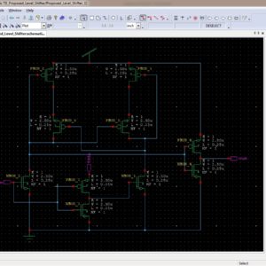
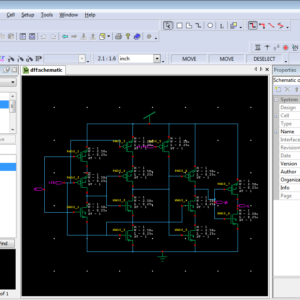
A Low Power and High Speed Voltage Level Shifter Based on a Regulated Cross Coupled Pull Up Network
Abstract:
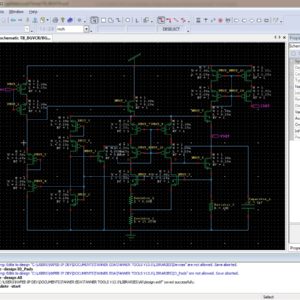
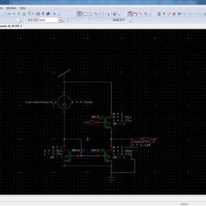
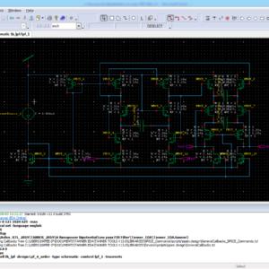
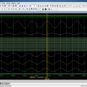
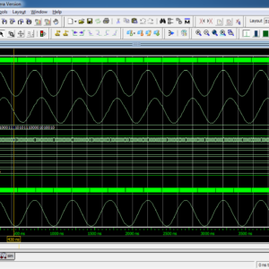
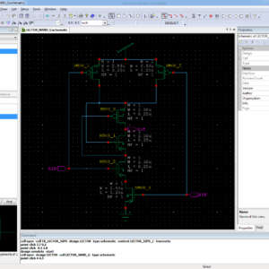
In this brief, a fast and very low power voltage level shifter (LS) is presented. By using a new regulated cross-coupled (RCC) pull-up network, the switching speed is boosted and the dynamic power consumption is highly reduced. The proposed (LS) has the ability to convert input signals with voltage levels much lower than the threshold voltage of a MOS device to higher nominal supply voltage levels. The presented LS occupies a small silicon area owing to its very low number of elements and is ultra-low-power, making it suitable for low-power applications such as implantable medical devices and wireless sensor networks. Results of the post-layout simulation in a standard 0.18-μm CMOS technology show that the proposed circuit can convert up input voltage levels as low as 80 mV. The power dissipation and propagation delay of the proposed level shifter for a low/high supply voltages of 0.4/1.8 V and input frequency of 1 MHz are 123.1 nW and 23.7 ns, respectively.
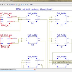
List of the following materials will be included with the Downloaded Backup:A High-Performance Multiply-Accumulate Unit by Integrating Additions and Accumulations into Partial Product Reduction Process
Abstract:
In this paper, we propose a low-power high-speed pipeline multiply-accumulate (MAC) architecture. In a conventional MAC, carry propagations of additions (including additions in multiplications and additions in accumulations) often lead to large power consumption and large path delay. To resolve this problem, we integrate a part of additions into the pa rtial product reduction (PPR) process. In the proposed MAC architecture, the addition and accumulation of higher significance bits are not performed until the PPR process of the next multiplication. To correctly deal with the overflow in the PPR process, a small-size adder is designed to accumulate the total number of carries. Compared with previous works, experimental results show that the proposed MAC architecture can greatly reduce both power consumption and circuit area under the same timing constraint.
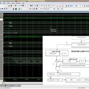
List of the following materials will be included with the Downloaded Backup:Low-Cost and Programmable CRC Implementation Based on FPGA
Abstract:
Cyclic redundancy check (CRC) is a well-known error detection code that is widely used in Ethernet, PCIe, and other transmission protocols. The existing FPGA-based implementation solutions encounter the problem of excessive resource utilization in high-performance scenarios. The padding zeros problem and the introduction of programmability further exacerbate this problem. In this brief, the stride-by-5 algorithm is proposed to achieve the optimal utilization of FPGA resources. The pipelining go back algorithm is proposed to solve the padding zeros problem. The method of reprogramming by HWICAP is proposed to realize programmability with small and constant resource utilization. The experimental results show that the resource utilization of the proposed non-segmented architecture is 80.7%-87.5% and 25.1%-46.2% lower than that of two state of-the-art FPGA-based CRC implementations, and the proposed segmented architecture has lower resource utilization, by 81.7%- 85.9% and 2.9%-20.8%, than two state-of-the-art architectures. Furthermore, throughput and programmability are guaranteed.
List of the following materials will be included with the Downloaded Backup:Design of ultra-low power consumption approximate 4-2 compressors based on the compensation characteristic
Abstract:
Approximate computing is tentatively applied in some digital signal processing applications which have an inherent tolerance for erroneous computing results. The approximate arithmetic blocks are utilized in them to improve the electrical performance of these circuits. Multiplier is one of the fundamental units in computer arithmetic blocks. Moreover, the 4-2 compressors are widely employed in the parallel multipliers to accelerate the compression process of partial products. In this paper, three novel approximate 4-2 compressors are proposed and utilized in 8-bit multipliers. Meanwhile, an error-correcting module (ECM) is presented to promote the error performance of approximate multiplier with the proposed 4-2 compressors. In this paper, the number of the approximate 4-2 compressor’s outputs is innovatively reduced to one, which brings further improvements in the energy efficiency. Compared with the exact 4-2 compressors, the simulation results indicate that the proposed approximate compressors UCAC1, UCAC2, UCAC3 achieve 24.76%, 51.43%, and 66.67% reduction in delay, 71.76%, 83.06%, and 93.28% reduction in power and 54.02%, 79.32%, and 93.10% reduction in area, respectively. And the utilization of these proposed compressors in 8-bit multipliers brings 49.29% reduction of power consumption on average.
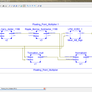
List of the following materials will be included with the Downloaded Backup:An Efficient Implementation of Floating Point Multiplier
Abstract:
In this paper we describe an efficient implementation of an IEEE 754 single precision floating point multiplier targeted for Xilinx Virtex-5 FPGA. VHDL is used to implement a technology-independent pipelined design. The multiplier implementation handles the overflow and underflow cases. Rounding is not implemented to give more precision when using the multiplier in a Multiply and Accumulate (MAC) unit. With latency of three clock cycles the design achieves 301 MFLOPs. The multiplier was verified against Xilinx floating point multiplier core.
List of the following materials will be included with the Downloaded Backup:FPGA implementation of low power and high speed image edge detection algorithm
Abstract:
Image processing is a vital task in data processing system for applications in medical fields, remote sensing, microscopic imaging etc., Algorithms for processing image exist except for real time system style, hardware implementation is most popular principally. This paper presents a design for Sobel filter based edge detection on Field Programmable Gate Array (FPGA) board. Hardware implementation of the Sobel edge detection algorithm is chosen because it presents an honest scope for similarity over software package. On the opposite hand, Sobel edge detection will work with less deterioration in high level of noise. Edges are primarily the noticeable variation of intensities in a picture. Edges facilitate to spot the placement of an object and also the boundary of a selected entity within the image. It conjointly helps in feature extraction and pattern recognition. Hence, edge detection is of nice importance in pc vision. The planned design for edge detection exploitation Sobel algorithm is designed using structural Verilog lipoprotein synthesized exploitation Cadence Genus and enforced using Cadence Innovus. The practicality of the planning is verified exploitation normal pictures by FPGA implementation. The proposed architecture reduce the power, delay and space complexity compare to three existing architectures.
List of the following materials will be included with the Downloaded Backup:A Design Implementation and Comparative Analysis of Advanced Encryption Standard (AES) Algorithm on FPGA
Abstract:
As the technology is getting advanced continuously the problem for the security of data is also increasing. The hackers are equipped with new advanced tools and techniques to break any security system. Therefore people are getting more concern about data security. The data security is achieved by either software or hardware implementations. In this work Field Programmable Gate Arrays (FPGA) device is used for hardware implementation since these devices are less complex, more flexible and provide more efficiency. This work focuses on the hardware execution of one of the security algorithms that is the Advanced Encryption Standard (AES) algorithm. The AES algorithm is executed on Vivado 2014.2 ISE Design Suite and the results are observed on 28 nanometers (nm) Artix-7 FPGA. This work discusses the design implementation of the AES algorithm and the resources consumed in implementing the AES design on Artix-7 FPGA. The resources which are consumed are as follows- Slice Register (SR), Look-Up Tables (LUTs), Input/Output (I/O) and Global Buffer (BUFG).
List of the following materials will be included with the Downloaded Backup:A Review on Fundamentals of Ternary Reversible Logic Circuits
Abstract:
One of the main motivations for using ternary logic systems is the amount of information per circuit line is higher as compared to the corresponding binary logic representation, thereby leading to more compact circuit realizations. This is particularly attractive for quantum computing as quarts are expensive resources and minimizing their number is one of the main objectives during synthesis. Therefore, ternary reversible logic synthesis has drawn significant attention among researchers. It deals with fundamental unit of information called quarts that can exist in one of the three states |0, |1 and |2. Hence, the aim of this paper is to bridge the knowledge gap for the beginners in this domain than searching the entire space. Therefore, the present work discusses the basic concepts of ternary reversible logic and ternary reversible gates. The detailed discussion of the various ternary reversible logic synthesis will enable the beginners in this domain to understand the ternary reversible logic in a better way.
List of the following materials will be included with the Downloaded Backup:High Speed Area Efficient VLSI Architecture of Three Operand Binary Adder
Abstract:
Three-operand binary adder is the basic functional unit to perform the modular arithmetic in various cryptography and pseudorandom bit generator (PRBG) algorithms. Carry save adder (CS3A) is the widely used technique to perform the three-operand addition. However, the ripple-carry stage in the CS3A leads to a high propagation delay of O(n). Moreover, a parallel prefix two-operand adder such as Han-Carlson (HCA) can also be used for three-operand addition that significantly reduces the critical path delay at the cost of additional hardware. Hence, a new high-speed and area-efficient adder architecture is proposed using pre-compute bitwise addition followed by carry prefix computation logic to perform the three-operand binary addition that consumes substantially less area, low power and drastically reduces the adder delay to O(log2 n). The proposed architecture is implemented on the FPGA device for functional validation and also synthesized with the commercially available 32nm CMOS technology library. The post-synthesis results of the proposed adder reported 3.12, 5.31 and 9.28 times faster than the CS3A for 32-, 64- and 128- bit architecture respectively. Moreover, it has a lesser area, lower power dissipation and smaller delay than the HC3A adder. Also, the proposed adder achieves the lowest ADP and PDP than the existing three-operand adder techniques.
List of the following materials will be included with the Downloaded Backup:Comparison and Extension of Approximate 4-2 Compressors for Low-Power Approximate Multipliers
Abstract:
Approximate multipliers attract a large interest in the scientific literature that proposes several circuits built with approximate 4-2 compressors. Due to the large number of proposed solutions, the designer who wishes to use an approximate 4-2 compressor is faced with the problem of selecting the right topology. In this paper, we present a comprehensive survey and comparison of approximate 4-2 compressors previously proposed in literature. We present also a novel approximate compressor, so that a total of twelve different approximate 4-2 compressors are analyzed. The investigated circuits are employed to design 8 × 8 and 16 × 16 multipliers, implemented in 28nm CMOS technology. For each operand size we analyze two multiplier configurations, with different levels of approximations, both signed and unsigned. Our study highlights that there is no unique winning approximate compressor topology since the best solution depends on the required precision, on the signedness of the multiplier and on the considered error metric.
List of the following materials will be included with the Downloaded Backup:Design and FPGA Implementation of Lattice Wave Digital Notch Filter with Minimal Transient Duration
Abstract:
In this study, the design and field-programmable gate array (FPGA) implementation of the digital notch filter with the lattice wave digital filter (LWDF) structure is presented. For reducing the initial signal transient, the variable notch bandwidth filter is designed. During the initial samples, the notch filter has a wide bandwidth in order to diminish signal transient. As time moves forward, the notch bandwidth reduces to attain the possible minimum width. This results in minimized transient duration notch filter with a sufficiently high-quality factor. Previously, the IIR structure has been used for implementing the time varying bandwidth notch filter. Such a filter requires two variable coefficients for varying the notch width with time. The advantage of using a LWDF structure is that only one coefficient has variable values to vary the notch width with time. Therefore, the number of memory locations required to implement the proposed design is reduced by half. Moreover, the LWDF is less sensitive to the word-length effects. Thus, the proposed lattice wave digital notch filter (LWDNF) produces better results compared to the existing literature in terms of error analysis. The suggested LWDNF is then implemented on a field-programmable gate array using a Xilinx system generator for the DSP design suite.
List of the following materials will be included with the Downloaded Backup:Design of a Scalable Low Power 1 bit Hybrid Full Adder for Fast Computation
Abstract:
A novel design of a hybrid Full Adder (FA) using Pass Transistors (PTs), Transmission Gates (TGs) and Conventional Complementary Metal Oxide Semiconductor (CCMOS) logic is presented. Performance analysis of the circuit has been conducted using Cadence toolset. For comparative analysis, the performance parameters have been compared with twenty existing FA circuits. The proposed FA has also been extended up to a word length of 64 bits in order to test its scalability. Only the proposed FA and five of the existing designs have the ability to operate without utilizing buffer in intermediate stages while extended to 64 bits. According to simulation results, the proposed design demonstrates notable performance in power consumption and delay which accounted for low power delay product. Based on the simulation results, it can be stated that the proposed hybrid FA circuit is an attractive alternative in the data path design of modern high-speed Central Processing Units.
List of the following materials will be included with the Downloaded Backup:High-Speed Hybrid-Logic Full Adder Using High-Performance 10-T XOR–XNOR Cell
Abstract:
Hybrid logic style is widely used to implement full adder (FA) circuits. Performance of hybrid FA in terms of delay, power, and driving capability is largely dependent on the performance of XOR–XNOR circuit. In this article, a high speed, low-power 10-T XOR–XNOR circuit is proposed, which provides full swing outputs simultaneously with improved delay performance. The performance of the proposed circuit is measured by simulating it in cadence virtuoso environment using 90-nm CMOS technology. The proposed circuit reduces the power delay product (PDP) at least by 7.5% than that of the available XOR–XNOR modules. Four different designs of FAs are also proposed in this article utilizing the proposed XOR–XNOR circuit and available sum and carry modules. The proposed FAs provide 2%–28.13% improvement in terms of PDP than that of other architectures. To measure the driving capabilities, the proposed FAs are embedded in 2-, 4-, and 8-bit cascaded full adder (CFA) structures. Results show that two of the proposed FAs provide the best performance for a higher number of bits among all the FAs.
List of the following materials will be included with the Downloaded Backup:An Efficient Design for Reversible Wallace Unsigned Multiplier
Abstract:
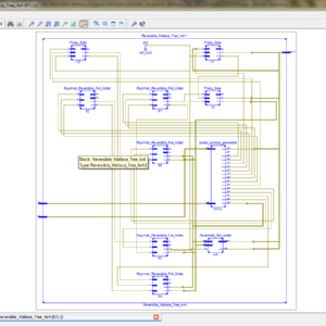
Today, reversible logic can be used for designing low-power CMOS circuits, optical data processing, DNA computations, biological researches, quantum circuits and nanotechnology. Sometimes using of reversible logic is inevitable such as build quantum computers. Reversible logic circuits structure is much more complicated than irreversible logic circuits. Multiplication operation is considered as one of the most important operations in the ALU unit. In this paper, we have proposed two 4×4 reversible unsigned multiplier circuits in which Wallace tree method is used to reduce the depth of circuits. In first design, the partial products circuit is designed using TG and FG gates so that TG is used to produce the partial products and FG for fan-out. In the second design, TG and PG gates are used to produce the partial products and no fan-out is required. Moreover, we have used PG gate and Feynman' block as reversible half-adder (HA) and full-adder (FA) in the summation network, respectively. In the first design, the main purpose is to decrease the depth of the circuit and increase the circuit speed. In the second design we would attempt to improve quantum parameters the number of garbage outputs, constant inputs and quantum cost. The evaluation results show that the first design, in terms of delay, is the fastest circuit. Also, the second design in terms of the number of constant inputs, garbage outputs and quantum cost is better than other designs.
List of the following materials will be included with the Downloaded Backup:Design and analysis of High speed Wallace tree multiplier using parallel prefix adders for VLSI circuit designs
Abstract:
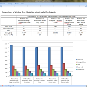
Major operation block in any processing unit is a multiplier. There are many multiplication algorithms are proposed, by using which multiplier structure can be designed. Among various multiplication algorithms, Wallace tree multiplication algorithm is beneficial in terms of speed of operation. With the advancement of technology, demand for circuits with high speed and low area is increasing. In order to improve the speed of Wallace tree multiplier without degrading its area parameter, a new structure of Wallace tree multiplier is proposed in this paper. In the proposed structure, the final addition stage of partial products is performed by parallel prefix adders (PPAs). In this paper, five Wallace tree multiplier structures are proposed using Kogge stone adder, Sklansky adder, Brent Kung adder, Ladner Fischer adder and Han carlson adder. All the multiplier structures are designed using Verilog HDL in Xilinix 13.2 design suite. The proposed structures are simulated using ISIM simulator and synthesized using XST synthesizer. The proposed designs are analyzed with respect to traditional multiplier design in terms of area (No. of LUTs) and delay (ns).
List of the following materials will be included with the Downloaded Backup:Low-Voltage Bandgap Reference Circuit in 28nm CMOS
Abstract:
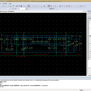
This paper presents a hybrid adjusted temperature compensation circuit for reducing the temperature drift of the bandgap reference. Combining first-order bandgap current, nonlinear compensation current, and temperature curvature compensation current together, a temperature insensitive reference voltage can be obtained in proposed circuit. Designed and verified in UMC 28nm CMOS technology with Cadence IC615, the proposed circuit achieves a post-layout simulation temperature drift of 5.48 ppm/°C in the range of -20°C to 120°C with a supply voltage of 1.05-V.
List of the following materials will be included with the Downloaded Backup:A Sub-200nW All-in-One Bandgap Voltage and Current Reference without Amplifiers
Abstract:
This brief presents a low-power and high-precision bandgap voltage and current reference (BGVCR) in one simple circuit for battery-powered applications. All the amplifiers have been eliminated in the proposed circuit. The voltage reference is derived from the bandgap topology, and the current reference is obtained by summing a proportional-to-absolute-temperature (PTAT) current and a complementary-to-absolute-temperature (CTAT) current. Therefore, the temperature coefficient of the current reference can be optimized. Besides, a pseudo-cascode structure and a simple line sensitivity enhancement circuit are adopted to improve the current mirror accuracy and line sensitivity. The proposed circuit is fabricated in a 0.18-μm deep N-well CMOS process with an active area of 0.063 mm2. The measured VREF and IREF are 1.2 V and 51 nA, respectively. The VREF and IREF show measured average temperature coefficients of 32.7 ppm/℃ and 89 ppm/℃ at a temperature of -45 to 125 ℃ and standard deviations of 0.17 % and 1.15 %, respectively. In the supply voltage range of 2 to 5 V, the line sensitivities of voltage and current are 0.058%/V and 1.76%/V, respectively. The minimum supply voltage is 2 V with a total power consumption of 192 nW at room temperature.
List of the following materials will be included with the Downloaded Backup:Area-Time Efficient Streaming Architecture for FAST and BRIEF Detector
Abstract:
The combination of FAST corners and BRIEF descriptors provide highly robust image features. We present a novel detector for computing the FAST-BRIEF features from streaming images. To reduce the complexity of the BRIEF descriptor, we employ an optimized adder tree to perform summation by accumulation on streaming pixels for the smoothing operation. Since the window buffer used in existing designs for computing the BRIEF point-pairs are often poorly utilized, we propose an efficient sampling scheme that exploits register reuse to minimize the number of registers. Synthesis results based on 65- nm CMOS technology show that the proposed FAST-BRIEF core achieves over 40% reduction in area-delay product compared to the baseline design. In addition, we show that the proposed architecture can achieve 1.4x higher throughput than the baseline architecture with slightly lower energy consumption.
List of the following materials will be included with the Downloaded Backup:AddNet: Deep Neural Networks Using FPGA-Optimized Multipliers
Abstract:
Low-precision arithmetic operations to accelerate deep-learning applications on field-programmable gate arrays (FPGAs) have been studied extensively, because they offer the potential to save silicon area or increase throughput. However, these benefits come at the cost of a decrease in accuracy. In this article, we demonstrate that reconfigurable constant coefficient multipliers (RCCMs) offer a better alternative for saving the silicon area than utilizing low-precision arithmetic. RCCMs multiply input values by a restricted choice of coefficients using only adders, subtractors, bit shifts, and multiplexers (MUXes), meaning that they can be heavily optimized for FPGAs. We propose a family of RCCMs tailored to FPGA logic elements to ensure their efficient utilization. To minimize information loss from quantization, we then develop novel training techniques that map the possible coefficient representations of the RCCMs to neural network weight parameter distributions. This enables the usage of the RCCMs in hardware, while maintaining high accuracy. We demonstrate the benefits of these techniques using AlexNet, ResNet-18, and ResNet-50 networks. The resulting implementations achieve up to 50% resource savings over traditional 8-bit quantized networks, translating to significant speedups and power savings. Our RCCM with the lowest resource requirements exceeds 6-bit fixed point accuracy, while all other implementations with RCCMs achieve at least similar accuracy to an 8-bit uniformly quantized design, while achieving significant resource savings.
List of the following materials will be included with the Downloaded Backup:Sparse FIR Filter Design via Partial 1-Norm Optimization
Abstract:
Electrocardiogram (ECG) is a form of cardiovascular measurement, for the diagnosis of different heart rate conditions. However, numerous noises usually harm the amplitude and time period of the signal from the ECG signal, at following a transition of the analog ECG signal from the sensor module into a digital format. The appropriate digital filter may be used to remove different forms of noise such as Baseline Wander, Power line interference, High frequency noise and Physiological Artifacts. The Digital FIR filter will have prospected to reduced the artifacts in the ECG signals. The signals taken from the MIT-BIH data base which contains the normal and abnormal waveforms. This Digital FIR filter can have more performance by using more TAP numbers such as multiplying, delaying and getting more effectiveness. This proposed work would implement a 1 norm minimization in the FIR filter with liner step method to minimize sparse complexity and reduce the mini-max approximation error for sparse maximization. Given these facts, several rules for selecting indicators of potential zero coefficients to be used in 1 standard optimization are adopted in the proposed algorithm. The efficacy of the proposed design algorithm was developed in Verilog HDL, simulated in Modelsim software and synthesized in Xilinx vertex 5 FPGA, and finally prove all the parameters in terms of area, delay and power.
List of the following materials will be included with the Downloaded Backup:A Compact 0.3 V Class AB Bulk Driven OTA
Abstract:
In this article, a new solution for an ultralow-voltage (ULV) ultralow-power (ULP) operational transconductance amplifier (OTA) is presented. Thanks to the combination of a low-voltage bulk-driven nontailed differential stage with the multipath Miller zero compensation technique, a simple class AB power-efficient ULV structure has been obtained, which can operate from supply voltages less than the threshold voltages of the employed MOS transistors, while offering rail-to-rail input common-mode range at the same time. The proposed OTA was fabricated using the 180-nm CMOS process from Taiwan Semiconductor Manufacturing Company (TSMC) and can operate from VDD ranging from 0.3 to 0.5 V. The 0.3-V version dissipates only 12.6 nW of power while showing a 64.7-dB voltage gain at 1-Hz, 2.96-kHz gain-bandwidth product, and a 4.15-V/ms average slew-rate at 30-pF load capacitance. The measured results agree well with simulations.
List of the following materials will be included with the Downloaded Backup:Area Delay and Energy Efficient Multi-Operand Binary Tree Adder
Abstract:
Here, the critical path of ripple carry adder (RCA)-based binary tree adder (BTA) is analyzed to find the possibilities for delay minimization. Based on the findings of the analysis, the new logic formulation and the corresponding design of RCA are proposed for the BTA. The comparison result shows that the proposed RCA design offers better efficiency in terms of area, delay and energy than the existing RCA. Using this RCA design, the BTA structure is proposed. The synthesis result reveals that the proposed 32-operand BTA provides the saving of 22.5% in area–delay product and 28.7% in energy–delay product over the recent Wallace tree adder which is the best among available multi-operand adders. The authors have also applied the proposed BTA in the recent multiplier designs to evaluate its performance. The synthesis result shows that the performance of multiplier designs improved significantly due to the use of proposed BTA. Therefore, the proposed BTA design can be a better choice to develop the area, delay and energy efficient digital systems for signal and image processing applications.
List of the following materials will be included with the Downloaded Backup:One-Sided Schmitt-Trigger-Based 9T SRAM Cell for Near-Threshold Operation
Abstract:
This paper presents a one-sided Schmitt-trigger based 9T static random access memory cell with low energy consumption and high read stability, write ability, and hold stability yields in a bit-interleaving structure without write-back scheme. The proposed Schmitt-trigger-based 9T static random access memory cell obtains a high read stability yield by using a one-sided Schmitt-trigger inverter with a single bit-line structure. In addition, the write ability yield is improved by applying selective power gating and a Schmitt-trigger inverter write assist technique that controls the trip voltage of the Schmitt-trigger inverter. The proposed Schmitt-trigger-based 9T static random access memory cell has 0.79, 0.77, and 0.79 times the area, and consumes 0.31, 0.68, and 0.90 times the energy of Chang’s 10T, the Schmitt-trigger-based 10T, and MH’s 9T static random access memory cells, respectively, based on 22-nm Fin FET technology.
List of the following materials will be included with the Downloaded Backup:Error Detection and Correction in SRAM Emulated TCAMs
Abstract:
Ternary content addressable memories (TCAMs) are widely used in network devices to implement packet classification. They are used, for example, for packet forwarding, for security, and to implement software-defined networks (SDNs). TCAMs are commonly implemented as standalone devices or as an intellectual property block that is integrated on networking application-specific integrated circuits. On the other hand, field-programmable gate arrays (FPGAs) do not include TCAM blocks. However, the flexibility of FPGAs makes them attractive for SDN implementations, and most FPGA vendors provide development kits for SDN. Those need to support TCAM functionality and, therefore, there is a need to emulate TCAMs using the logic blocks available in the FPGA. In recent years, a number of schemes to emulate TCAMs on FPGAs have been proposed. Some of them take advantage of the large number of memory blocks available inside modern FPGAs to use them to implement TCAMs. A problem when using memories is that they can be affected by soft errors that corrupt the stored bits. The memories can be protected with a parity check to detect errors or with an error correction code to correct them, but this requires additional memory bits per word. In this brief, the protection of the memories used to emulate TCAMs is considered. In particular, it is shown that by exploiting the fact that only a subset of the possible memory contents are valid, most single-bit errors can be corrected when the memories are protected with a parity bit.
List of the following materials will be included with the Downloaded Backup:A Highly Efficient Conditional Feed through Pulsed Flip Flop for High Speed Applications
Abstract:
A novel type of highly efficient conditional feed through pulse-triggered flip-flop (P-FF) is proposed and demonstrated. The data-to-output (D-to-Q) delay in this circuit was highly optimized using pre discharging and conditional signal feed through schemes. Power consumption was also reduced using a shared pulse generator and an output feedback-controlled conditional keeper, which diminished the floating status of the internal node. The driving strength of this design was further enhanced by including an additional pull-down path at the output node. Various post layout simulation results applied to 16-nm Fin FET technology demonstrated a higher energy efficiency (at all input data toggle rates) for the proposed topology than comparable P-FF devices. Notably, the proposed model achieved a 62% D-to-Q delay reduction, compared to a transmission gate FF, outperforming the device by more than 66% in terms of power efficiency and 87% in energy efficiency (at a 50% input data toggle rate). Improvements were even more significant in comparison with other conventional P-FFs. These results suggest the proposed design to be a viable new option for high-efficiency sequential elements in high-speed applications.
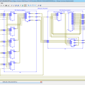
List of the following materials will be included with the Downloaded Backup:ER-TCAM: A Soft-Error-Resilient SRAM-Based Ternary Content-Addressable Memory for FPGAs
Abstract:
Static random access memory (SRAM)-based ternary content-addressable memory (TCAM) on field-programmable gate arrays (FPGAs) is used for packet classification in software-defined networking (SDN) and Open Flow applications. SRAMs implementing TCAM contents constitute the major part of a TCAM design on FPGAs, which are vulnerable to soft errors. The protection of SRAM-based TCAMs against soft errors is challenging without compromising critical path delay and maintaining a high search performance. This brief presents a low cost and low-response-time technique for the protection of SRAM-based TCAMs. This technique uses simple, single-bit parity for fault detection which has a minimal critical path overhead. This technique exploits the binary-encoded TCAM table maintained in SRAM-based TCAMs for update purposes to implement a low-response-time error-correction mechanism at low cost. The error-correction process is carried out in the background, allowing lookup operations to be performed simultaneously, thus maintaining a high search performance. The proposed technique provides protection against soft errors with a response time of 293 ns, whereas maintaining a search rate of 222 million searches per second on a 1024 × 40 size TCAM on Artix-7 FPGA.
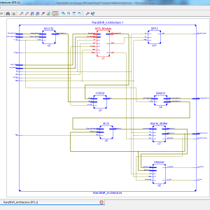
List of the following materials will be included with the Downloaded Backup:RandShift: An Energy-Efficient Fault Tolerant Method in Secure Nonvolatile Main Memory
Abstract:
In this article, we present a simple, yet energy- and area-efficient method for tolerating the stuck-at faults caused by an endurance issue in secure-resistive main memories. In the proposed method, by employing the random characteristics of the encrypted data encoded by the Advanced Encryption Standard (AES) as well as a rotational shift operation, a large number of memory locations with stuck-at faults could be employed for correctly storing the data. Due to the simple hardware implementation of the proposed method, its energy consumption is considerably smaller than that of other recently proposed methods. The technique may be employed along with other error correction methods, including the error correction code (ECC) and the error correction pointer (ECP). To assess the efficacy of the proposed method, it is implemented in a phase-change memory (PCM)- based main memory system and compared with three error tolerating methods. The results reveal that for a stuck-at fault occurrence rate of 10−2 and with the uncorrected bit error rate of 2 × 10⁻³, the proposed method achieves 82% energy reduction compared to the state-of-the-art method. More generally, using a simulation analysis technique, we show that the fault coverage of the proposed method is similar to that of the state-of-the-art method.
List of the following materials will be included with the Downloaded Backup:Feed forward-Cutset-Free Pipelined Multiply–Accumulate Unit for the Machine Learning Accelerator
Abstract:
Multiply–accumulate (MAC) computations account for a large part of machine learning accelerator operations. The pipelined structure is usually adopted to improve the performance by reducing the length of critical paths. An increase in the number of flip-flops due to pipelining, however, generally results in significant area and power increase. A large number of flip-flops are often required to meet the feed forward-cutset rule. Based on the observation that this rule can be relaxed in machine learning applications, we propose a pipelining method that eliminates some of the flip-flops selectively. The simulation results show that the proposed MAC unit achieved a 20% energy saving and a 20% area reduction compared with the conventional pipelined MAC.
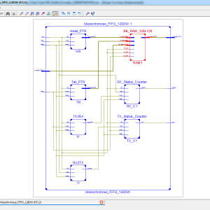
List of the following materials will be included with the Downloaded Backup:The Mesochronous Dual-Clock FIFO Buffer
Abstract:
To increase system composability and facilitate timing closure, fully synchronous clocking is replaced by more relaxed clocking schemes, such as mesochronous clocking. Under this regime, the modules at the two ends of a mesochronous interface receive the same clock signal, thus operating under the same clock frequency, but the edges of the arriving clock signals may exhibit an unknown phase relationship. In such cases, clock synchronization is needed when sending data across modules. In this brief, we present a novel mesochronous dual-clock first-input– first-output (FIFO) buffer that can handle both clock synchronization and temporary data storage, by synchronizing data implicitly through the explicit synchronization of only the flow-control signals. The proposed design can operate correctly even when the transmitter and the receiver are separated by a long link whose delay cannot fit within the target operating frequency. In such scenarios, the proposed mesochronous FIFO can be extended to support multicycle link delays in a modular manner and with minimal modifications to the baseline architecture. When compared with the other state-of-the-art dual-clock mesochronous FIFO designs, the new architecture is demonstrated to yield a substantially lower cost implementation.
List of the following materials will be included with the Downloaded Backup:FPGA Based True Random Number Generation Using Programmable Delays in Oscillator Rings
Abstract:
True random number generators play a fundamental role in cryptographic systems. This paper presents a new and efficient method to generate true random numbers on field programmable gate array by utilizing the random jitter of free running oscillators as a source of randomness. The free-running oscillator rings incorporate programmable delay lines to generate large variation of the oscillations and to introduce jitter in the generated ring oscillators clocks. The main advantage of the proposed true random number generator utilizing programmable delay lines is to reduce correlation between several equal length oscillator rings, and thus improve the randomness qualities. In addition, a Von Neumann corrector as post-processor is employed to remove any bias in the output bit sequence. The validation of the proposed approach is demonstrated on Xilinx Spartan-3A FPGAs. The proposed true random number generator occupies 528 slices, achieves 6 Mbps throughput with 0.999 per bit entropy rate, and passes all the National Institute of Standards and Technology (NIST) statistical tests.
List of the following materials will be included with the Downloaded Backup:Vital-Sign Processing Receiver With Clutter Elimination Using Servo Feedback Loop for UWB Pulse Radar System
Abstract:
This brief presents a vital-sign processing circuit for simultaneous dc/near-dc elimination and out-of-band interference rejection without any digital signal processing or algorithm assistance for the ultra wideband (UWB) pulse-based radar system. An intrinsic self balanced MOS diode (SBMD) was proposed as a stable and balanced pseudo resistor applied under a servo feedback loop in a vital-sign receiver of the sensing radar to perform as a high-pass filter (HPF) with an ultralow corner frequency lower than 0.5 Hz for removing undesired clutters of the reflected signals and input dc-offset voltages from innate circuit offsets. A third-order switched-capacitor (SC) Chebyshev low-pass filter (LPF) with leap-frog topology as the subsequent stage was adopted to suppress the out-band noises, thereby establishing an integrated vital-sign processing circuit with band pass frequency response and incorporating it into a radar module to verify its viability.
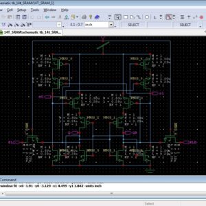
List of the following materials will be included with the Downloaded Backup:Radiation-Hardened 0.3–0.9-V Voltage-Scalable 14T SRAM and Peripheral Circuit in 28-nm Technology for Space Applications
Abstract:
Conventional radiation-hardened cells of static random access memory (SRAM) are not robust enough in 28 nm technology, due to partial immunity of single-event upset (SEU) effect (Quatrobased cells) or insufficient critical charges in sensitive nodes (conventional stacked cells). The reduction of read noise margin (RNM) at the low supply voltage (VDD) confines these cells from low VDD applications. We propose a novel interleaving stacked-14T (ILS-14T) cell which prevents voltage transient from propagating to other redundancies. The ILS-14T cell can be resilient to both 0–1 and 1–0 upsets by injecting 12 mA in sensitive nodes. The critical charges of the ILS-14T cell are substantially larger than most other hardened cells at VDD from 0.3 to 0.9 V. The RNM of the ILS-14T cell is two times of most Quatro-based cells at 0.3 V VDD and larger than most cells at 0.6 and 0.9 V VDD. The area of occupation is 334% of the conventional 6T cell, which equals other 14T cells. The static–dynamic decoder array with 20%–40% area penalty and 116%–132% delay of rising edge, when compared with the conventional one, reduces the read failure rate by preventing single event transients (SETs) from propagating to unexpected word lines (WLs).
List of the following materials will be included with the Downloaded Backup:FPGA-Based System For Heart Rate Monitoring
Abstract:
The continuous monitoring of cardiac patients requires an ambulatory system that can automatically detect heart diseases. This study presents a new field programmable gate array (FPGA)-based hardware implementation of the QRS complex detection. The proposed detection system is mainly based on the Pan and Tompkins algorithm, but applying a new, simple, and efficient technique in the detection stage. The new method is based on the centred derivative and the intermediate value theorem, to locate the QRS peaks. The proposed architecture has been implemented on FPGA using the Xilinx System Generator for digital signal processor and the Nexys-4 FPGA evaluation kit. To evaluate the effectiveness of the proposed system, a comparative study has been performed between the resulting performances and those obtained with existing QRS detection systems, in terms of reliability, execution time, and FPGA resources estimation. The proposed architecture has been validated using the 48 half-hours of records obtained from the Massachusetts Institute of Technology - Beth Israel Hospital (MITBIH) arrhythmia database. It has also been validated in real time via the analogue discovery device.
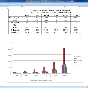
List of the following materials will be included with the Downloaded Backup:A Two-Speed, Radix-4, Serial–Parallel Multiplier (Booth Multiplier )
Abstract:
In this paper, we present a two-speed, radix-4, serial-parallel multiplier for accelerating applications such as digital filters, artificial neural networks, and other machine learning algorithms. Our multiplier is a variant of the serial–parallel (SP) modified radix-4 Booth multiplier that adds only the nonzero Booth encodings and skips over the zero operations, making the latency dependent on the multiplier value. Two sub circuits with different critical paths are utilized so that throughput and latency are improved for a subset of multiplier values. The multiplier is evaluated on an Intel Cyclone V field-programmable gate array against standard parallel–parallel and SP multipliers across four different process–voltage–temperature corners. We show that for bit widths of 32 and 64, our optimizations can result in a 1.42×–3.36× improvement over the standard parallel Booth multiplier in terms of area–time depending on the input set.
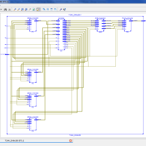
List of the following materials will be included with the Downloaded Backup:Efficient TCAM Design Based on Multipumping Enabled Multiported SRAM on FPGA
Abstract:
Ternary content-addressable memory (TCAM)-based search engines play an important role in networking routers. The search space demands of TCAM applications are constantly rising. However, existing realizations of TCAM on field-programmable gate arrays (FPGAs) suffer from storage inefficiency. This paper presents a multipumping-enabled multiported SRAM-based TCAM design on FPGA, to achieve an efficient utilization of SRAM memory. Existing SRAM-based solutions for TCAM reduce the impact of the increase in the traditional TCAM pattern width from an exponential growth in memory usage to a linear one using cascaded block RAMs (BRAMs) on FPGA. However, BRAMs on state-of-the-art FPGAs have a minimum depth limitation, which limits the storage efficiency for TCAM bits. Our proposed solution avoids this limitation by mapping the traditional TCAM table divisions to shallow sub-blocks of the configured BRAMs, thus achieving a memory-efficient TCAM memory design. The proposed solution operates the configured simple dual-port BRAMs of the design as multiported SRAM using the multipumping technique, by clocking them with a higher internal clock frequency to access the sub-blocks of the BRAM in one system cycle. We implemented our proposed design on a Virtex-6 xc6vlx760 FPGA device. Compared with existing FPGA-based TCAM designs, our proposed method achieves up to 2.85 times better performance per memory.
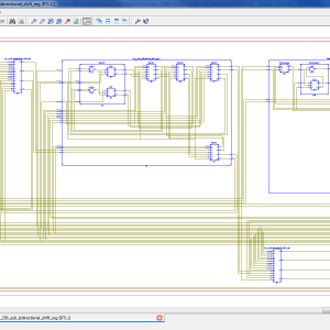
List of the following materials will be included with the Downloaded Backup:Area-Efficient Bidirectional Shift-Register Using Bidirectional Pulsed-Latches
Abstract:
This paper proposes an area-efficient bidirectional shift-register using bidirectional pulsed-latches. The proposed bidirectional shift-register reduces the area and power consumption by replacing master-slave flip-flops and 2-to-1 multiplexers with the proposed bidirectional pulsed-latches and non-overlap delayed pulsed clock signals, and by using sub shift-registers and extra temporary storage latches. A 256-bit bidirectional shift-register was fabricated using a 65nm CMOS process. Its area was 1,943μm2 and its power consumption is 200μW at a 100MHz clock frequency with VDD=1.2V. It reduces area by 39.2% and power consumption by 19.4% compared to the conventional bidirectional shift-register, length in most cases.
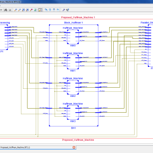
List of the following materials will be included with the Downloaded Backup:A High-Throughput Hardware Accelerator for Lossless Compression of a DDR4 Command Trace
Abstract:
In a memory system, understanding how the host is stressing the memory is important to improve memory performance. Accordingly, the need for the analysis of memory command trace, which the memory controller sends to the dynamic random access memory, has increased. However, the size of this trace is very large; consequently, a high-throughput hardware (HW) accelerator that can efficiently compress these data in real time is required. This paper proposes a high throughput HW accelerator for lossless compression of the command trace. The proposed HW is designed in a pipeline structure to process Huffman tree generation, encoding, and stream merge. To avoid the HW cost increase owing to high throughput processing, a Huffman tree is efficiently implemented by utilizing static random access memory-based queues and bitmaps. In addition, variable length stream merge is performed at a very low cost by reducing the HW wire width using the mathematical properties of Huffman coding and processing the metadata and the Huffman codeword using FIFO separately. Furthermore, to improve the compression efficiency of the DDR4 memory command, the proposed design includes two preprocessing operations, the “don’t care bits override” and the “bits arrange,” which utilize the operating characteristics of DDR4 memory. The proposed compression architecture with such preprocessing operations achieves a high throughput of 8 GB/s with a compression ratio of 40.13% on average. Moreover, the total HW resource per throughput of the proposed architecture is superior to the previous implementations.
List of the following materials will be included with the Downloaded Backup:Highly Linear Low-Power Wireless RF Receiver for WSN
Abstract:
This paper introduces a low-power wireless RF receiver for the wireless sensor network. The receiver has improved linearity with incorporated current-mode circuits and high-selectivity filtering. The receiver operates at the 900-MHz industrial, scientific, and medical band and is implemented in 130-nm CMOS technology. The receiver has a frequency multiplication mixer, which uses a 300-MHz clock from a local oscillator (LO). The LO is implemented using vertical delay cells to reduce power consumption. The receiver conversion gain is 40 dB and the receiver noise. The receiver’s input third-order intercept point (IIP3) is −6 dBm and the total power consumption is 1.16 mW.
List of the following materials will be included with the Downloaded Backup:A 13.4-MHz Relaxation Oscillator With Temperature Compensation
Abstract:
A low-phase-noise relaxation oscillator uses a digital compensation loop to reduce its temperature coefficient (TC). This relaxation oscillator is fabricated in the 0.18-µm CMOS process. The measured average oscillation frequency is 13.4 MHz. The whole oscillator consumes 157.8 µW under a 1.2-V supply. The measured average TCs of the oscillation frequency with and without compensation are 193.15 and 1098.7 ppm/◦C, respectively. The TC achieves an improvement of 5.7 times. The measured frequency variation is within ±2% from −20 ◦C to 100 ◦C by using the digital compensation loop. The measured phase noise at 100-kHz offset frequency is −104.82 dBc/Hz, and the measured figure of merit (FOM) is −154.4 dBc/Hz
List of the following materials will be included with the Downloaded Backup:Design of Sparse FIR Filters With Reduced Effective Length
Abstract:
In this paper, an exchange algorithm is proposed to design sparse linear phase finite impulse response (FIR) filters with reduced effective length. The sparse FIR filter design problem is formally an l0-norm minimization problem. This original design problem is re-formulated by encoding the filter coefficients using a binary encoding vector, which represents the locations of the zero and non-zero filter coefficients. An iterative 0-1 exchange process with proper direction control is proposed to propel the minimax approximation error toward the specified upper bound of error for sparsity maximization. The effective length is optimized with a lower priority than sparsity in the proposed algorithm. Simulation results show that the proposed algorithm is superior to the existing algorithms in terms of both sparsity and/or effective length in most cases.
List of the following materials will be included with the Downloaded Backup:Column-Selection-Enabled 10T SRAM Utilizing Shared Diff-VDD Write and Dropped-VDD Read for Power Reduction
Abstract:
A non-destructive column-selection-enabled 10T SRAM for aggressive power reduction is presented in this brief. It frees a half-selected behavior by exploiting the bit line-shared data-aware write scheme. The differential-VDD (Diff-VDD) technique is adopted to improve the write ability of the design. In addition, its decoupled read bit lines are given permission to be charged and discharged depending on the stored data bits. In combination with the proposed dropped-VDD biasing, it achieves the significant power reduction. The experimental results show that the proposed design provides the 3.3× improvement in the write margin compared with the standard Diff-10T SRAM. A 5.5-kb 10T SRAM in a 65-nm CMOS process has a total power of 51.25 µW and a leakage power of 41.8 µW when operating at 6.25 MHz at 0.5 V, achieving 56.3% reduction in dynamic power and 32.1% reduction in leakage power compared with the previous single-ended 10T SRAM.
List of the following materials will be included with the Downloaded Backup:Instantaneous Power Consuming Level Shifter for Improving Power Conversion Efficiency of Buck Converter
Abstract:
An instantaneous power consuming level shifter is presented in this paper to increase the DC converter efficiency. The level shifter is used in a high-side power switch driver to remove the external capacitor which is used in bootstrap technique. The level shifter consumes power only during the transition period. A delay cell is used to turn the level shifter off to reduce the power consumption period. An output voltage detector is added to turn the level shifter off even before the delay time. An asynchronous discontinuous conduction mode buck converter is designed to verify the performance of the level shifter. Simulation results show that the power consumption of the proposed level shifter decreased by 66%, while the converter efficiency increased by the maximum of 9% compared to results obtained for a conventional level shifter. The converter is fabricated using the TSMC 0.18-µm BCD process and it operates within an input range of 2–5 V when the current varies from 400 µA to 18 mA and delivers an output voltage of 1.8 V.
List of the following materials will be included with the Downloaded Backup:Many-Objective Sizing Optimization of a Class-C/D VCO for Ultralow-Power IoT and Ultralow Phase-Noise Cellular Applications
Abstract:
In this paper, the performance boundaries and corresponding tradeoffs of a complex dual-mode class-C/D voltage controlled oscillator (VCO) are extended using a framework for the automatic sizing of radio frequency integrated circuit blocks, where an all-inclusive test bench formulation enhanced with an additional measurement processing system enables the optimization of “everything at once” toward its true optimal tradeoffs. VCOs embedded in the state-of-the-art multi standard transceivers must comply with extremely high performance and ultralow power requirements for modern cellular and Internet of Things applications. However, the proper analysis of the design tradeoffs is tedious and impractical, as a large amount of conflicting performance figures obtained from multiple modes, test benches, and/or analysis must be considered simultaneously. Here, the dual-mode design and optimization conducted provided 287 design solutions with figures of merit above 192 dBc/Hz, where the power consumption varies from 0.134 to 1.333 mW, the phase noise at 10 MHz from −133.89 to −142.51 dBc/Hz, and the frequency pushing from 2 to 500 MHz/V, on the worst case of the tuning range. These results pushed this circuit design to its performance limits on a 65-nm CMOS technology, reducing 49% of the power consumption of the original design while also showing its potential for ultralow power with more than 93% reduction. In addition, worst case corner criteria were also performed on the top of the worst case tuning range optimization, taking the problem to a human-untrea table LXVI-D performance space.
List of the following materials will be included with the Downloaded Backup:A 7T Security Oriented SRAM Bitcell
Abstract:
Power analysis (PA) attacks have become a serious threat to security systems by enabling secret data extraction through the analysis of the current consumed by the power supply of the system. Embedded memories, often implemented with six-transistor (6T) static random access memory (SRAM) cells, serve as a key component in many of these systems. However, conventional SRAM cells are prone to side-channel power analysis attacks due to the correlation between their current characteristics and written data. To provide resiliency to these types of attacks, we propose a security-oriented 7T SRAM cell, which incorporates an additional transistor to the original 6T SRAM implementation and a two-phase write operation, which significantly reduces the correlation between the stored data and the power consumption during write operations. The proposed 7T SRAM cell was implemented in a 28 nm technology and demonstrates over 1000× lower write energy standard deviation between write ‘1’ and ‘0’ operations compared to a conventional 6T SRAM. In addition, the proposed cell has a 39%–53% write energy reduction and a 19%–38% reduced write delay compared to other power analysis resistant SRAM cells.
List of the following materials will be included with the Downloaded Backup:Energy-Quality Scalable Adders Based on Non-zeroing Bit Truncation
Abstract:
Approximate addition is a technique to trade off energy consumption and output quality in error-tolerant applications. In prior art, bit truncation has been explored as a lever to dynamically trade off energy and quality. In this brief, an innovative bit truncation strategy is proposed to achieve more graceful quality degradation compared to state-of-the-art truncation schemes. This translates into energy reduction at a given quality target. When applied to a ripple-carry adder, the proposed bit truncation approach improves quality by up to 8.5 dB in terms of peak signal-to-noise ratio, compared to traditional bit truncation. As a case study, the proposed approach was applied to a discrete cosine transform engine. In comparison with prior art, the proposed approach reduces energy by 20%, at insignificant delay and silicon area overhead.
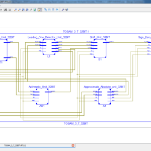
List of the following materials will be included with the Downloaded Backup:TOSAM: An Energy-Efficient Truncation- and Rounding-Based Scalable Approximate Multiplier
Abstract:
A scalable approximate multiplier, called truncation- and rounding-based scalable approximate multiplier (TOSAM) is presented, which reduces the number of partial products by truncating each of the input operands based on their leading one-bit position. In the proposed design, multiplication is performed by shift, add, and small fixed-width multiplication operations resulting in large improvements in the energy consumption and area occupation compared to those of the exact multiplier. To improve the total accuracy, input operands of the multiplication part are rounded to the nearest odd number. Because input operands are truncated based on their leading one-bit positions, the accuracy becomes weakly dependent on the width of the input operands and the multiplier becomes scalable. Higher improvements in design parameters (e.g., area and energy consumption) can be achieved as the input operand widths increase. To evaluate the efficiency of the proposed approximate multiplier, its design parameters are compared with those of an exact multiplier and some other recently proposed approximate multipliers. Results reveal that the proposed approximate multiplier with a mean absolute relative error in the range of 11%–0.3% improves delay, area, and energy consumption up to 41%, 90%, and 98%, respectively, compared to those of the exact multiplier. It also outperforms other approximate multipliers in terms of speed, area, and energy consumption. The proposed approximate multiplier has an almost Gaussian error distribution with a near-zero mean value. We exploit it in the structure of a JPEG encoder, sharpening, and classification applications. The results indicate that the quality degradation of the output is negligible. In addition, we suggest an accuracy configurable TOSAM where the energy consumption of the multiplication operation can be adjusted based on the minimum required accuracy.
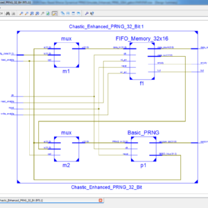
List of the following materials will be included with the Downloaded Backup:Chaos-Based Bitwise Dynamical Pseudorandom Number Generator on FPGA
Abstract:
In this paper, a new pseudorandom number generator (PRNG) based on the logistic map has been proposed. To prevent the system to fall into short period orbits as well as increasing the randomness of the generated sequences, the proposed algorithm dynamically changes the parameters of the chaotic system. This PRNG has been implemented in a vertex 7 field-programmable gate array (FPGA) with a 32-bit fixed point precision, using a total of 510 lookup tables (LUTs) and 120 registers. The sequences generated by the proposed algorithm have been subjected to the National Institute of Standards and Technology (NIST) randomness tests, passing all of them. By comparing the randomness with the sequences generated by a raw 32-bit logistic map, it is shown that, by using only an additional 16% of LUTs, the proposed PRNG obtains a much better performance in terms of randomness, increasing the NIST passing rate from 0.252 to 0.989. Finally, the proposed bitwise dynamical PRNG is compared with other chaos-based realizations previously proposed, showing great improvement in terms of resources and randomness.
List of the following materials will be included with the Downloaded Backup:World’s Fastest FFT Architectures: Breaking the Barrier of 100 GS/s
Abstract:
This paper presents the fastest fast Fourier transform (FFT) hardware architectures so far. The architectures are based on a fully parallel implementation of the FFT algorithm. In order to obtain the highest throughput while keeping the resource utilization low, we base our design on making use of advanced shift-and-add techniques to implement the rotators and on selecting the most suitable FFT algorithms for these architectures. Apart from high throughput and resource efficiency, we also guarantee high accuracy in the proposed architectures. For the implementation, we have developed an automatic tool that generates the architectures as a function of the FFT size, input word length and accuracy of the rotations. We provide experimental results covering various FFT sizes, FFT algorithms, and field-programmable gate array boards. These results show that it is possible to break the barrier of 100 GS/s for FFT calculation.
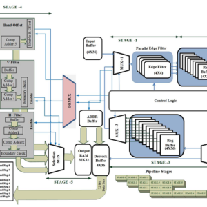
List of the following materials will be included with the Downloaded Backup:Design and Implementation of Efficient Streaming Deblocking and SAO Filter for HEVC Decoder
We have also Code for 720 x 576 Image Resolution using 64 x 64 Block Size of HEVC. Cost of this Update work in High Resolution Rs. 45,000/- ( Rs. 45,000/- + Rs. 35,000/- ) : Total Cost : Rs. 80,000/-
Abstract:
This paper aims to design an efficient mixed serial five-stage pipeline processing hardware architecture of deblocking filter (DBF) and sample adaptive offset (SAO) filter for high efficiency video coding decoder. The proposed hardware is designed to increase the throughput and reduce the number of clock cycles by processing the pixels in a stream of 4 × 36 samples in which edge filters are applied vertically in a parallel fashion for processing of luma/chroma samples. Subsequently these filtered pixels are transposed and reprocessed through vertical filter for horizontal filtering in a pipeline fashion. Finally, the filtered block transposed back to the original orientation and forwarded to a three-stage pipeline SAO filter. The proposed architecture is implemented in field programmable gate array and application specific integrated circuit platform using 90-nm library. Experimental results illustrate that the proposed DBF and SAO architecture decreases the processing cycles (172) required for processing each 64 × 64 or large coding unit compared with the state-of-the-art literature with the increase of gate count (593.32K) including memory. The results show that the throughput of the proposed filter can successfully decode ultrahigh definition video sequences at 200 frames/s at 341 MHz.
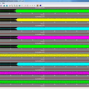
List of the following materials will be included with the Downloaded Backup:A System of Two Coupled Oscillators With a Continuously Controllable Phase Shift
Abstract:
We present a novel generalization of quadrature oscillators (QVCO) which we call “arbitrary phase oscillator” or APO for short. In contrast to a QVCO which generates only quadrature phases, the APO is capable of continuously generating any desired phase at its output. The proposed structure employs a novel coupling mechanism to generate arbitrary phase shifts between two coupled oscillators without the need for an explicit phase shifter. A rigorous nonlinear dynamic analysis is presented to give a closed-form formula for the generated phase shifts, and the theory is verified by numerical simulation as well as measurement results of a prototype chip fabricated in 130-nm CMOS technology. The prototype APO has a frequency tuning range of 4.90–5.65 GHz and is continuously phase tunable from 0◦ to 360◦ across the entire frequency range. The APO structure can be used in designing novel coupled-oscillator-based phased arrays for 5G wireless communications.
List of the following materials will be included with the Downloaded Backup:A High Resolution FPGA TDC Converter with 2.5 ps Bin Size and -3.79~6.53 LSB Integral Non linearity
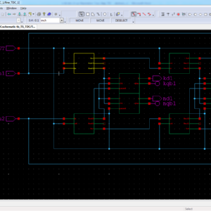
Abstract:
As a traditional digital platform, Field Programmable Gate Array (FPGA) is seldom used for analog applications. Since there is no way to fine tune the gate property or circuit structure, the performance of FPGA analog application is usually inferior to its counterparts based on full-custom or even cell-based design. Nevertheless, a high performance FPGA time-to-digital Converter (TDC) is proposed in this paper to expand the FPGA territory into high-end analog applications. The test time signal is sampled by a serious timing references generated by feeding the original clock into a tapped delay line. According to periodicity, the delays among those timing references are wrapped into a single reference period and the effective TDC resolution can be made much smaller than the clock period to compete even with the state-of the art full-custom TDCs in performance. After measurement, the effective resolution is as fine as 2.5 ps. The corresponding differential nonlinearity (DNL) is -1.90~1.66 LSB and the integral nonlinearity (INL) is -3.79~6.53 LSB only.
List of the following materials will be included with the Downloaded Backup:Analysis, Comparison, and Experimental Validation of a Class AB Voltage Follower With Enhanced Bandwidth and Slew Rate
Abstract:
This paper describes a bandwidth (BW)- and slew rate (SR)-enhanced class AB voltage follower (VF). A thorough small signal analysis of the proposed and a state-of-the-art AB-enhanced VF is presented to compare their performance. The proposed circuit has 50-MHz BW, 19.5-V/µs SR, and a BW figure of merit of 41.6 (MHz × pF/µW) for CL = 50 pF. It provides 13 times higher current efficiency and 15 times higher BW than the conventional VF with equal 60-µW static power dissipation. The experimental and simulation results of a fabricated test chip in the 130-nm CMOS technology validate the proposed circuit.
List of the following materials will be included with the Downloaded Backup:A 16-bit 2.0-ps Resolution Two-Step TDC in 0.18-μm CMOS Utilizing Pulse-Shrinking Fine Stage
Abstract:
This paper proposes a time-to-digital converter (TDC) that achieves wide input range and fine time resolution at the same time. The proposed TDC utilizes pulse-shrinking (PS) scheme in the second stage for a fine resolution and two-step (TS) architecture for a wide range. The proposed PS TDC prevents an undesirable non-uniform shrinking rate issue in the conventional PS TDCs by utilizing a built-in offset pulse and an offset pulse width detection schemes. With several techniques, including a built-in coarse gain calibration mechanism, the proposed TS architecture overcomes a nonlinearity due to the signal propagation and gain mismatch between coarse and fine stages. The simulation results of the TDC implemented in a 0.18-µm standard CMOS technology demonstrate 2.0-ps resolution and 16-bit range that corresponds to ∼130-ns input time interval with 0.08-mm2 area. It operates at 3.3 MS/s with 18.0 mW from 1.8-V supply and achieves 1.44-ps single-shot precision. Index Terms— Built-in calibration, pulse shrinking (PS), time-to-digital conversion, two step (TS).
List of the following materials will be included with the Downloaded Backup:A Nanopower Biopotential Lowpass Filter Using Subthreshold Current-Reuse Biquads With Bulk Effect Self-Neutralization
Abstract:
A nanopower CMOS 4th-order lowpass filter suitable for biomedical applications is presented. The filter is formed by cascading two types of subthreshold current-reuse biquadratic cell. Each proposed cell is capable of neutralizing the bulk effect that induces the passband attenuation. The nearly 0-dB passband gain can thus be maintained, while the entire filter circuit remains compact and power-efficient. Designed for electrocardiogram detection as an example of application, the filter prototype has been fabricated in a 0.35 µm CMOS process occupying 269 µm × 383 µm chip area. Measurements verify that the filter can operate from a 1.5-V single supply and consumes 5.25 nW, while providing a cutoff frequency of 100 Hz and input-referred noise of 39.38 µVrms. The intermodulation-free dynamic range of 51.48 dB is obtained from a two-tone test of 50 and 60 Hz input frequencies. Compared with state-of-the-art nanopower lowpass filters using the most relevant and reasonable figure of merit, the proposed filter ranks the best.
List of the following materials will be included with the Downloaded Backup:Low-Complexity 2-D Digital FIR Filters Using Polyphase Decomposition and Farrow Structure
Abstract:
This paper proposes a novel realization technique for quadrantally symmetric 2-D finite impulse response filters with a guaranteed reduction in the hardware complexity. Here, the concept of Farrow structure-based interpolation filter design using the polyphase decomposition of the 1-D filter transfer function is effectively utilized in the 2-D domain. The proposed 2-D filter makes use of row-wise polyphase decomposition of the 2-D transfer function or frequency response, followed by the polynomial approximation of the individual polyphase coefficients resulting in Farrow structures corresponding to each row filter. The final coefficients are implemented by varying the delay values in all the Farrow structures, followed by the interpolation of the coefficients obtained from each delay value, which in turn forms the rows in the 2-D kernel. The major highlight of the proposed method is the highly reduced implementation complexity in terms of the number of multipliers and adders, with a low normalized root-mean-square error. Design examples of the circularly symmetric and fan-type filters have been considered to show the efficiency of the approach. The results show a drastic reduction in the implementation complexity of the 2-D filters of upto 20%, with significantly low normalized root-mean-square error lesser than 0.5%.
List of the following materials will be included with the Downloaded Backup:Static Delay Variations Modules For Ripple-Carry and Borrow Save Adders
Abstract:
This paper introduces two statistical delay variability models for certain hardware adder implementations, namely, the ripple-carry adder (RCA) and the borrow-save adder (BSA). The introduced models take into account correlated variation sources. Initially, we derive a first proposed model, namely, Type-I model, in the form of expressions for the computation of the exact Probability Density Functions (PDFS) of maximum output delays for Gaussian and non-Gaussian variation sources. Furthermore, we present closed formulas for the co-variances between output delays of the aforementioned adder architectures. The introduced derived co-variances are subsequently combined with Clark’s method to derive a second proposed model, Type-II model, which comprises approximations of the maximum delay PDF for an RCA and a BSA. Simulation results and the derived exact Type-I PDFs are found to perfectly agree, while the proposed Clark-based Type-II models present an error for standard deviation of maximum delay that increases as BSA word length increases. Both the introduced models and the simulations prove that BSAs achieve narrower delay distributions than RCAs, i.e., they significantly reduce delay variance. Consequently, BSAs are proven to be suitable for variation-tolerant applications by providing a timing safety margin, when compared to RCA architectures. The underlying analysis indicates that for the case of BSA and either intra-die delay variations only or both intra and inter-die delay variations, the Type-II models introduce non negligible errors, which are as much as 16% of the standard deviation of maximum delay for a 256-digit BSA, as the Type II Gaussian PDF approximations deviate significantly from the exact Type-I PDFs. However, for all RCA and BSA inter-die only variation cases, both types present satisfactory accuracy due to the Gaussian shape of exact PDF.
List of the following materials will be included with the Downloaded Backup:New Majority Gate Based Parallel BCD Adder Designs for Quantum-dot Cellular Automata
Abstract:
In this paper, we first theoretically re-defined output decimal carry in terms of majority gates and proposed a carry look ahead structure for calculating all the intermediate output carries. We have used this method for designing the multi-digit decimal adders. Theoretically, our best n-digit decimal adder design reduces the delay and area-delay product (ADP) by 50% compared with previous designs. We have implemented our designs using QCA Designer tool. The proposed QCA Designer based 8-digit PBA-BCD adder achieves over 38% less delay compared with the best existing designs.
List of the following materials will be included with the Downloaded Backup:VLSI Design of SVM-Based Seizure Detection System With On-Chip Learning Capability
Abstract:
Portable automatic seizure detection system is very convenient for epilepsy patients to carry. In order to make the system on-chip trainable with high efficiency and attain high detection accuracy, this paper presents a very large scale integration (VLSI) design based on the nonlinear support vector machine (SVM). The proposed design mainly consists of a feature extraction (FE) module and an SVM module. The FE module performs the three level Daubechies discrete wavelet transform to fit the physiological bands of the electroencephalogram (EEG) signal and extracts the time–frequency domain features reflecting the non stationary signal properties. The SVM module integrates the modified sequential minimal optimization algorithm with the table-driven-based Gaussian kernel to enable efficient on-chip learning. The presented design is verified on an Altera Cyclone II field-programmable gate array and tested using the two publicly available EEG datasets. Experiment results show that the designed VLSI system improves the detection accuracy and training efficiency.
List of the following materials will be included with the Downloaded Backup:A Low Complexity I/Q Imbalance Calibration Method for Quadrature Modulator
Abstract:
This brief presents a low-complexity I/Q (in-phase and quadrature components) imbalance calibration method for the transmitter using quadrature modulation. Impairments in analog quadrature modulator have a deleterious effect on the signal fidelity. Among the critical impairments, I/Q imbalance (gain and phase mismatches) deteriorates the residual sideband performance of the analog quadrature modulator degrading the error vector magnitude. Based on the theoretical mismatch analysis of the quadrature modulator, we propose a low-complexity I/Q imbalance extraction algorithm. After the parameter extraction, the transmitter is calibrated by imposing the counter imbalanced mismatch of the transmitter through the digital baseband. In comparison with existing I/Q imbalance calibration methods, the novelty of the proposed method lies in that: 1) only three spectrum measurements of the device-under-test are needed for extraction and calibration of gain and phase mismatches; 2) due to the blind nature of the calibration algorithm, the proposed approach can be readily applicable to an existing I/Q transmitter; 3) no extra hardware that degrades the calibration accuracy is required; and 4) due to the non-iterative nature, the proposed method is faster and computationally more efficient than previously published methods.
List of the following materials will be included with the Downloaded Backup:Low-Power Near-Threshold 10T SRAM Bit Cells With Enhanced Data-Independent Read Port Leakage for Array Augmentation in 32-nm CMOS
Abstract:
The conventional six-transistor static random access memory (SRAM) cell allows high density and fast differential sensing but suffers from half-select and read-disturb issues. Although the conventional eight-transistor SRAM cell solves the read-disturb issue, it still suffers from low array efficiency due to deterioration of read bit-line (RBL) swing and Ion/Ioff ratio with increase in the number of cells per column. Previous approaches to solve these issues have been afflicted by low performance, data dependent leakage, large area, and high energy per access. Therefore, in this paper, we present three iterations of SRAM bit cells with nMOS-only based read ports aimed to greatly reduce data dependent read port leakage to enable 1k cells/RBL, improve read performance, and reduce area and power over conventional and 10T cell-based works. We compare the proposed work with other works by recording metrics from the simulation of a 128-kb SRAM constructed with divided-word line-decoding architecture and a 32-bit word size. Apart from large improvements observed over conventional cells, up to 100-mV improvement in read-access performance, up to 19.8% saving in energy per access, and up to 19.5% saving in the area are also observed over other 10T cells, thereby enlarging the design and application gamut for memory designers in low-power sensors and battery-enabled devices.
List of the following materials will be included with the Downloaded Backup:Energy-Efficient Approximate Multiplier Design using Bit Significance-Driven Logic Compression
Abstract:
Approximate arithmetic has recently emerged as a promising paradigm for many imprecision-tolerant applications. It can offer substantial reductions in circuit complexity, delay and energy consumption by relaxing accuracy requirements. In this paper, we propose a novel energy-efficient approximate multiplier design using a significance-driven logic compression (SDLC) approach. Fundamental to this approach is an algorithmic and configurable lossy compression of the partial product rows based on their progressive bit significance. This is followed by the commutative remapping of the resulting product terms to reduce the number of product rows. As such, the complexity of the multiplier in terms of logic cell counts and lengths of critical paths is drastically reduced. A number of multipliers with different bit-widths (4-bit to 128-bit) are designed in System Verilog and synthesized using Synopsys Design Compiler. Post-synthesis experiments showed that up to an order of magnitude energy savings, and reductions of 65% in critical delay and almost 45% in silicon area can be achieved for a 128-bit multiplier compared to an accurate equivalent. These gains are achieved with low accuracy losses estimated at less than 0.00071 mean relative error. Additionally, we demonstrate the energy-accuracy trade-offs for different degrees of compression, achieved through configurable logic clustering. In evaluating the effectiveness of our approach, a case study image processing application showed up to 68.3% energy reduction with negligible losses in image quality expressed as peak signal-to-noise ratio (PSNR).
List of the following materials will be included with the Downloaded Backup:Low-Power Approximate Unsigned Multipliers with Configurable Error Recovery
Abstract:
Approximate circuits have been considered for applications that can tolerate some loss of accuracy with improved performance and/or energy efficiency. Multipliers are key arithmetic circuits in many of these applications including digital signal processing (DSP). In this paper, a novel approximate multiplier with a low power consumption and a short critical path is proposed for high-performance DSP applications. This multiplier leverages a newly designed approximate adder that limits its carry propagation to the nearest neighbors for fast partial product accumulation. Different levels of accuracy can be achieved by using either OR gates or the proposed approximate adder in a configurable error recovery. The multipliers using these two error reduction strategies are referred to as approximate multiplier 1 (AM1) and approximate multiplier 2 (AM2), respectively. Both AM1 and AM2 have a low mean error distance, i.e., most of the errors are not significant in magnitude. Compared to a Wallace multiplier optimized for speed, an 8×8 AM1 with 4 MSBs (most significant bits) for error reduction and synthesized using a 28 nm CMOS process shows a 60% reduction in delay (when optimized for delay) and a 42% reduction in power dissipation (when optimized for area). In a 16×16 design, half of the least significant partial products are truncated for AM1 and AM2, which are thus denoted as TAM1 and TAM2, respectively. Compared with the Wallace multiplier, TAM1 and TAM2 save from 50% to 66% in power, when optimized for area. Compared to existing approximate multipliers, AM1, AM2, TAM1 and TAM2 show significant advantages in accuracy with a high performance. AM2 has a better accuracy compared to AM1 but with a longer delay and higher power consumption. Image processing applications including image sharpening and smoothing are considered to show the quality of the approximate multipliers in error-tolerant applications. By utilizing an appropriate error recovery, the proposed approximate multipliers achieve similar processing accuracy as traditional exact multipliers, but with significant improvements in power.
List of the following materials will be included with the Downloaded Backup:A Real-Time FHD Learning Based Super Resolution System Without a Frame Buffer
Abstract:
The main aim of the Single image (SR) super-resolution is to generate (HR) high-resolution images from (LR) low-resolution images. This paper briefly presents a concept of real time super resolution method of FHD based image extended and scaling processor. The super resolution system includes three blocks of operations. The first is a low-frequency interpolation stage, where bicubic interpolation is used for reconstructing the low-frequency parts of HR images. The second stage generates high-frequency patches by choosing the highest related pre-trained regression function according to each HR low frequency patch. In the third stage, with the high-frequency information, the low-frequency image patches are enhanced and overlapped to construct the SR result. These operations for gaining a high-frequency result are applied to the Y-luminance channel only, while the high-resolution Cb and Cr channels are generated by bicubic interpolation. The proposed system generates the output image resolution of 1920 X 1080 (FHD) by the input of 800 X 800 image size. The proposed architecture performs an anchored neighborhood regression algorithm that generates a high-resolution image from a low-resolution image input using only numbers of line buffers. Finally, super resolution technique is implemented in VHDL and Synthesized in the XILINX VERTEX-5 FPGA and shown the comparison for power, area and delay reports.
List of the following materials will be included with the Downloaded Backup:A 0.3-V 37-nW 53-dB SNDR Asynchronous Delta–Sigma Modulator in 0.18-μm CMOS
Abstract:
A new solution for an ultralow-voltage bulk driven (BD) asynchronous delta–sigma modulator is described in this paper. While implemented in a standard 0.18-µm CMOS process from the Taiwan Semiconductor Manufacturing Company and supplied with VDD = 0.3 V, the circuit offers a 53.3-dB signal-to-noise and distortion ratio, which corresponds to 8.56-bit resolution. In addition, the total power consumption is 37 nW, the signal bandwidth is 62 Hz, and the resulting power efficiency is 0.79 pJ/conversion. The above-mentioned features have been achieved employing a highly linear transconductor and a hysteretic comparator based on nontailed BD differential pair.
List of the following materials will be included with the Downloaded Backup:Line Coding Techniques for Channel Equalization: Integrated Pulse-Width Modulation and Consecutive Digit Chopping
Abstract:
This paper presents two new line-coding schemes, integrated pulse width modulation (iPWM) and consecutive digit chopping (CDC) for equalizing lossy wire line channels with the aim of achieving energy efficient wire line communication. The proposed technology friendly encoding schemes are able to overcome the fundamental limitations imposed by Manchester or pulse-width modulation encoding on high-speed wire line transceivers. A highly digital encoder architecture is leveraged to implement the proposed iPWM and CDC encoding. Energy-efficient operation of the proposed encoding is demonstrated on a high-speed wire line transceiver that can operate from 10 to 18 Gb/s. Fabricated in a 65-nm CMOS process, the transceiver operates with supply voltages of 0.9 V, 1 V, and 1.1 V. With the help of the proposed iPWM encoding, the transceiver can equalize over 27-dB of channel loss while operating at 16 Gb/s with an efficiency of 4.37 pJ/bit. The design occupies an active die area of 0.21 mm2.
List of the following materials will be included with the Downloaded Backup:An LUT Based RNS FIR Filter Implementation for Reconfigurable Applications
Abstract:
In this work, two approaches to realize a look up table (LUT) based finite impulse response (FIR) filter using Residue Number System (RNS) are proposed. The proposed implementations take advantage of shift and add approach offered by the chosen module set. The two proposed filter architecture are compared with an earlier proposed version of reconfigurable RNS FIR filter. The filters are synthesized using Cadence RTL compiler in UMC 90 nm technology. The performance of the filters are compared in terms of Area (A), Power (P), and Delay (T). The results show that one of the proposed architecture offers significant improvement in terms of delay, while the second approach is well suited for applications that require minimal power and area. Both implementations offer advantage in area delay and power-delay-product. Proposed approaches are also verified functionally using Altera DSP Builder.
List of the following materials will be included with the Downloaded Backup:Radiation-Hardened 14T SRAM Bit cell With Speed and Power Optimized for Space Application
Abstract:
In this paper, a novel radiation-hardened 14-transistor SRAM bit cell with speed and power optimized [radiation-hardened with speed and power optimized (RSP)-14T] for space application is proposed. By circuit- and layout-level optimization design in a 65-nm CMOS technology, the 3-D TCAD mixed-mode simulation results show that the novel structure is provided with increased resilience to single-event upset as well as single-event–multiple-node upsets due to the charge sharing among OFF-transistors. Moreover, the HSPICE simulation results show that the write speed and power consumption of the proposed RSP-14T are improved by ∼65% and ∼50%, respectively, compared with those of the radiation hardened design (RHD)-12T memory cell.
List of the following materials will be included with the Downloaded Backup:A Combined Deblocking Filter and SAO Hardware Architecture for HEVC
Abstract:
The latest video coding standard high-efficiency video coding (HEVC) provides 50% improvement in coding efficiency compared to H.264/AVC to meet the rising demands for video streaming, better video quality, and higher resolution. The deblocking filter (DF) and sample adaptive offset (SAO) play an important role in the HEVC encoder, and the SAO is newly adopted in HEVC. Due to the high throughput requirement in the video encoder, design challenges such as data dependence, external memory traffic, and on-chip memory area become even more critical. To solve these problems, we first propose an interlacing memory organization on the basis of quarter-LCU to resolve the data dependence between vertical and horizontal filtering of DF. The on-chip SRAM area is also reduced to about 25% on the basis of quarter-LCU scheme without throughput loss. We also propose a simplified bitrate estimation method of rate-distortion cost calculation to reduce the computational complexity in the mode decision of SAO. Our proposed hardware architecture of combined DF and SAO is designed for the HEVC intraencoder, and the proposed simplified bitrate estimation method of SAO can be applied to both intra- and intercoding. As a result, our design can support ultrahigh definition 7680 × 4320 at 40 f/s applications at merely 182 MHz working frequency. Total logic gate count is 103.3 K in 65 nm CMOS process.
List of the following materials will be included with the Downloaded Backup:CMOS First-Order All-Pass Filter With 2-Hz Pole Frequency
Abstract:
A CMOS fully integrated all-pass filter with an extremely low pole frequency of 2 Hz is introduced in this paper. It has 0.08-dB passband ripple and 0.029-mm2Si area. It has 0.38-mW power consumption in strong inversion with ±0.6-V power supplies. In subthreshold, it has 0.64-µW quiescent power and operates with ±200-mV dc supplies. Miller multiplication is used to obtain a large equivalent capacitor without excessive Si area. By varying the gain of the Miller amplifier, the pole frequency can be varied from 2 to 48 Hz. Experimental and simulation results of a test chip prototype in 130-nm CMOS technology validate the proposed circuit.
List of the following materials will be included with the Downloaded Backup:A Decoder for Short BCH Codes With High Decoding Efficiency and Low Power for Emerging Memories
Abstract:
In this paper, a double-error-correcting and triple error-detecting (DEC-TED) Bose–Chaudhuri–Hocquenghem (BCH) code decoder with high decoding efficiency and low power for error correction in emerging memories is presented. To increase the decoding efficiency, we propose an adaptive error correction technique for the DEC-TED BCH code that detects the number of errors in a codeword immediately after syndrome generation and applies a different error correction algorithm depending on the error conditions. With the adaptive error correction technique, the average decoding latency and power consumption are significantly reduced owing to the increased decoding efficiency. To further reduce the power consumption, an invalid-transition-inhibition technique is proposed to remove the invalid transitions caused by glitches of syndrome vectors in the error-finding block. Synthesis results with an industry-compatible 65-nm technology library show that the proposed decoders for the (79, 64, 6) BCH code take only 37%–48% average decoding latency and achieve more than 70% power reduction compared to the conventional fully parallel decoder under the 10−4–10−2 raw bit-error rate.
List of the following materials will be included with the Downloaded Backup:Design of Reconfigurable Digital IF Filter with Low Complexity
Abstract:
Due to limited frequency resources, new services are being applied to the existing frequencies, and service providers are allocating some of the existing frequencies for newly enhanced mobile communications. Because of this frequency environment, repeater and base station systems for mobile communications are becoming more complicated, and frequency interference caused by multiple bands and services is getting worse. Therefore, a heterodyne receiver using IF filters with high selectivity has been used to minimize the interference between frequencies. However, repeater and base station systems in mobile communications employing fixed IF filters cannot actively cope with the usage of multiple frequency bands, the application of various services, and frequency recycling. Therefore, this brief proposes a reconfigurable digital IF filter with variable center frequency and bandwidth while achieving high selectivity as existing IF filters. The center frequency of filter can vary from 10MHz to 62.5MHz, and the filter bandwidth can be selective to one of 10MHz, 15MHz, and 20MHz. The proposed digital filter also reduces the complexity of adders and multipliers by 38.81% and 41.57%, respectively, compared to an existing digital filter by using a filter bank and a multi stage structure. This digital IF filter is fabricated on a 130-nm CMOS process and occupies 5.90 mm2.
List of the following materials will be included with the Downloaded Backup:Multiloop Control for Fast Transient DC–DC Converter
Abstract:
A novel ac coupled feedback (ACCF) is proposed to alternatively realize fast transient response while inherently controlling the start-up in-rush current of a dc–dc switching converter. The proposed ACCF is modified from a conventional capacitor multiplier and connected between the outputs of the converter and the transconductance. With this supplemental feedback, the transient response has been significantly improved due to the gain-boosting effect around the compensator’s midband. Moreover, the ACCF circuit assists to manage the ramping speed of the output voltage during power-up, thereby eliminating the bulky soft-start circuit. The new controller is very simple to implement and occupies a tiny footprint on-chip. A buck converter with the proposed scheme has been fabricated using the 0.18-µm standard CMOS process with an active silicon area of 0.573 mm2. Measurement results show that the output voltage rises linearly for a soft-start period of 1.05 ms according to the designed slope. Excellent load transient responses are achieved under different load current steps; the output voltage overshoot/undershoot of 60 mV settles down within 10 µs for a load variation from 50 µA to 1 A in 1 µs. Moreover, the proposed converter maintains both excellent load and line regulations of 0.018 mV/mA and 0.0056 mV/mV, respectively.
List of the following materials will be included with the Downloaded Backup:A Novel Design of Flip-Flop Circuits using Quantum Dot Cellular Automata (QCA)
Abstract:
As the device dimension is shrinking day by day the conventional transistor based CMOS technology encounters serious hindrances due to the physical barriers of the technology such as ultra-thin gate oxides, short channel effects, leakage currents & excessive power dissipation at nano scale regimes. Quantum Dot Cellular Automata is an alternate challenging quantum phenomenon that provides a completely different computational platform to design digital logic circuits using quantum dots confined in the potential well to effectively process and transfer information at nano level as a competitor of traditional CMOS based technology. This paper has demonstrated the implementation of circuits like D, T and JK flip flops using a derived expression from SR flip-flop. The kink energy and energy dissipations has been calculated to determine the robustness of the designed flip-flops. The simulation results have been verified using QCA Designer simulation tool.
List of the following materials will be included with the Downloaded Backup:An Analog LO Harmonic Suppression Technique for SDR Receivers
Abstract:
A low-complexity analog technique to suppress the local oscillator (LO) harmonics in software-defined radios is presented. Accurate mathematical analyses show that an effective attenuation of the LO harmonics is achieved by modulating the transconductance of the low-noise transconductance amplifier (LNTA) with a raised-cosine signal. This modulation is performed through the bias network of a cascode device with a negligible increase in the LNTA noise figure. The proposed technique results in a notch at the third harmonic and at least 36 dB of attenuation at the fifth and the seventh harmonics. Experimental results in 130-nm CMOS and post layout simulation results in 65-nm CMOS verify the proper functionality of the proposed technique and the accuracy of the proposed analyses
List of the following materials will be included with the Downloaded Backup:Low Power and High Speed Implementation of FIR filter design using CMOS GDI Truncated Multiplier
Abstract:
The logic size, propagation delay, power of applications, based upon this improvement the adder design logic size will reduced year by year, here a proposed In recent technology of any application, adders is a more priority to do a function and task of arithmetic operation, in crucial this adder based arithmetic operation will decide work of this paper will design using a single bit full adder to design a multiplier. In this multiplier design, adder is a main priority to reduce the arithmetic logic size and increases speed of multiplier, in recent we have lots of multiplier design, Vedic multiplier, Wallace tree multiplier, booth multiplier, approximate multiplier. Here, the proposed work will taken truncated multiplier design, it's because, the truncated multiplier will have a capability to reduced internal and external architecture size in every design, regarding this truncated multiplier will have three options such as rounding, deleting, truncating, here the MSB bits will be truncated and present the output of n x n multiplication will provided only n bit level, using this truncated multiplier the proposed work will designed a 8-Tap FIR(Finite impulse response) filter and shown the efficiency of filter design using this CMOS GDI (Gate Diffusion Input) adder design. This proposed work will design in CMOS Logic gate and which 10-T transistor level of full adders with 90um technology, finally proved the terms of area, delay and power.
List of the following materials will be included with the Downloaded Backup:Design of Area-Efficient and Highly Reliable RHBD 10T Memory Cell for Aerospace Applications
Abstract:
In this brief, based on upset physical mechanism together with reasonable transistor size, a robust 10T memory cell is first proposed to enhance the reliability level in aerospace radiation environment, while keeping the main advantages of small area, low power, and high stability. Using Taiwan Semiconductor Manufacturing Company 65-nmCMOS commercial standard process, simulations performed in Cadence Spectre demonstrate the ability of the proposed radiation-hardened-by-design 10T cell to tolerate both 0 →1and1→0 single node upsets, with the increased read/write access time.
List of the following materials will be included with the Downloaded Backup:Towards Efficient Modular Adders based on Reversible Circuits
Abstract:
Reversible logic is a computing paradigm that has attracted significant attention in recent years due to its properties that lead to ultra-low power and reliable circuits. Reversible circuits are fundamental, for example, for quantum computing. Since addition is a fundamental operation, designing efficient adders is a cornerstone in the research of reversible circuits. Residue Number Systems (RNS) has been as a powerful tool to provide parallel and fault-tolerant implementations of computations where additions and multiplications are dominant. In this paper, for the first time in the literature, we propose the combination of RNS and reversible logic. The parallelism of RNS is leveraged to increase the performance of reversible computational circuits. Being the most fundamental part in any RNS, in this work we propose the implementation of modular adders, namely modulo 2n-1 adders, using reversible logic. Analysis and comparison with traditional logic show that modulo adders can be designed using reversible gates with minimum overhead in comparison to regular reversible adders.
List of the following materials will be included with the Downloaded Backup:Efficient Super Resolution Algorithm using Overlapping Bi-cubic Interpolation
Abstract:
In practical CCTV applications, there are problems of the camera with low resolution, camera fields of view, and lighting environments. These could degrade the image quality and it is difficult to extract useful information for further processing. Super-resolution techniques have been proposed widely by the researchers. However, many approaches are complex and are difficult to use in practical scenarios. In this paper, we propose an efficient Super-resolution algorithm using overlapping bi-cubic for hardware implementation. Experimental results are verified using processing time and reconstructed images that can be used in real time applications.
List of the following materials will be included with the Downloaded Backup:FIR Filter Design based on FPGA
Abstract:
FIR (Finite Impulse Response) Filters: the finite impulse response filter is the most basic components in digital signal processing systems are widely used in communications, image processing, and pattern recognition. Based on FPGA(editable logic device) to achieve FIR filter, not only take into account the fixed -function DSP-specific chip real-time, but also has the DSP processor flexibility. The combination of FPGA and DSP technology can further improve integration, increase work speed and expand system capabilities.
List of the following materials will be included with the Downloaded Backup:Gate diffusion input based 4-bit Vedic multiplier design
Abstract:
A multiplier is one of the key hardware blocks in most of the processors. Multiplication is a lengthy, time-consuming task. Vedic multiplication in field programmable gate array implementation has been proven effective in reducing the number of steps and circuit delay. Conventionally at the circuit level, complementary metal oxide semiconductor (CMOS) logic is used to design a multiplier. In CMOS circuits, the area is always an issue. Gate diffusion input (GDI)-based logic has been explored in the literature to reduce the number of transistors for various logic functions. Thus, Vedic mathematics, on the one hand, simplifies the multiplication process and reduces the delay; while on the other hand, GDI technique helps in minimizing the transistor count (TC) and reduction in power. Therefore, this study puts forth a GDI logic-based 4-bit Vedic multiplier. To study the effectiveness of the GDI logic, the transient response of a 2-bit Vedic multiplier using CMOS and GDI is compared. For the 4-bit Vedic multiplier, two design approaches are taken into consideration. The performance of these circuits is analyzed in terms of average power dissipation, delay, and TC. The effect of supply voltage scaling is also studied. The circuit simulations are carried out at 130 nm for bulk metal oxide semiconductor field effect transistor predictive technology model-based device parameters.
List of the following materials will be included with the Downloaded Backup:Efficient Design for Fixed-Width Adder-Tree
Abstract:
Conventionally, fixed-width adder-tree (AT) design is obtained from the full-width AT design by employing direct or post-truncation. In direct-truncation, one lower order bit of each adder output of full-width AT is post-truncated, and in case of post-truncation, {p} lower order-bits of final-stage adder output are truncated, where p = dlog2 Ne and N is the input-vector size. Both these methods do not provide an efficient design. In this paper, a novel scheme is presented to obtain fixed-width AT design using truncated input. A bias estimation formula based on probabilistic approach is presented to compensate the truncation error. The proposed fixed-width AT design for input-vector sizes 8 and 16 offers (37%, 23%, 22%) and (51%, 30%, 27%) area delay product (ADP) saving for word-length sizes (8, 12, 16), respectively, and calculates the output almost with the same accuracy as the post-truncated fixed-width AT which has the highest accuracy among the existing fixed-width AT. Further, we observed that Walsh-Hadamard transform based on the proposed fixed-width AT design reconstruct higher-texture images with higher peak signal to noise ratio (PSNR) and moderate-texture images with almost the same PSNR compared to those obtained using the existing AT designs. Besides, the proposed design creates an additional advantage to optimize other blocks appear at the upstream of the AT in a complex design.
List of the following materials will be included with the Downloaded Backup:LECTOR: A Technique for Leakage Reduction in CMOS Circuits
Abstract:
In CMOS circuits, the reduction of the threshold voltage due to voltage scaling leads to increase in sub threshold leakage current and hence static power dissipation. We propose a novel technique called LECTOR for designing CMOS gates which significantly cuts down the leakage current without increasing the dynamic power dissipation. In the proposed technique, we introduce two leakage control transistors (a p-type and a n-type) within the logic gate for which the gate terminal of each leakage control transistor (LCT) is controlled by the source of the other. In this arrangement, one of the LCTs is always “near its cutoff voltage” for any input combination. This increases the resistance of the path from to ground, leading to significant decrease in leakage currents. The gate-level net list of the given circuit is first converted into a static CMOS complex gate implementation and then LCTs are introduced to obtain a leakage-controlled circuit. The significant feature of LECTOR is that it works effectively in both active and idle states of the circuit, resulting in better leakage reduction compared to other techniques. Further, the proposed technique overcomes the limitations posed by other existing methods for leakage reduction. Experimental results indicate an average leakage reduction of 79.4% for MCNC’91 benchmark circuits.
List of the following materials will be included with the Downloaded Backup:High speed and low power preset-able modified TSPC D flip-flop design and performance comparison with TSPC D flip-flop
Abstract:
Positron emission tomography (PET) is a nuclear functional imaging technique that produces a three-dimensional image of functional organs in the body. PET requires high resolution, fast and low power multichannel analog to digital converter (ADC). A typical multichannel ADC for PET scanner architecture consists of several blocks. Most of the blocks can be designed by using fast, low power D flip-flops. A preset-able true single phase clocked (TSPC) D flip-flop shows numerous glitches (noise) at the output due to unnecessary toggling at the intermediate nodes. Preset-able modified TSPC (MTSPC) D flip flop have been proposed as an alternative solution to alleviate this problem. However, the MTSPC D flip-flop requires one extra PMOS to suspend toggling of the intermediate nodes. In this work, we designed a 7-bit preset-able gray code counter by using the proposed D flip-flop. This work involves UMC 180 nm CMOS technology for preset-able 7-bit gray code counter where we achieved 1 GHz maximum operation frequency with most significant bit (MSB) delay 0.96 ns, power consumption 244.2 μW (micro watt) and power delay product (PDP) 0.23 pJ (Pico joule) from 1.8 V power supply.
List of the following materials will be included with the Downloaded Backup:An Efficient VLSI Architecture for Convolution Based DWT Using MAC
Abstract:
The modern real time applications related to image processing and etc., demand high performance discrete wavelet transform (DWT). This paper proposes the floating point multiply accumulate circuit (MAC) based 1D/2D-DWT, where the MAC is used to find the outputs of high/low pass FIR filters. The proposed technique is implemented with 45 nm CMOS technology and the results are compared with various existing techniques. The proposed 8 × 8-point floating point 2-levels 2D-DWT achieves 27.6% and 83.7% of reduction in total area and net power respectively as compared with existing DWT.
List of the following materials will be included with the Downloaded Backup:Design of Low Power High Performance 2-4 and 4-16 Mixed-Logic Line Decoders
Abstract:
This paper introduces a mixed-logic design method for line decoders, combining transmission gate logic, pass transistor dual-value logic and static CMOS. Two novel topologies are presented for the 2-4 decoders: a 14-transistor topology aiming on minimizing transistor count and power dissipation and a 15-transistor topology aiming on high power delay performance. Both a normal and an inverting decoder are implemented in each case, yielding a total of four new designs. Furthermore, four new 4-16 decoders are designed, by using mixed-logic 2-4 pre decoders combined with standard CMOS post-decoder. All proposed decoders have full swinging capability and reduced transistor count compared to their conventional CMOS counterparts. Finally, a variety of comparative spice simulations at the 32 nm shows that the proposed circuits present a significant improvement in power and delay, outperforming CMOS in almost all cases.
List of the following materials will be included with the Downloaded Backup:A Floating-Point Fused Dot-Product Unit
Abstract:
A floating-point fused dot-product unit is presented that performs single-precision floating-point multiplication and addition operations on two pairs of data in a time that is only 150% the time required for a conventional floating-point multiplication. When placed and routed in a 45nm process, the fused dot-product unit occupied about 70% of the area needed to implement a parallel dot-product unit using conventional floating-point adders and multipliers. The speed of the fused dot-product is 27% faster than the speed of the conventional parallel approach. The numerical result of the fused unit is more accurate because one rounding operation is needed versus at least three for other approaches.
List of the following materials will be included with the Downloaded Backup:HDL-Based Modeling Approach for Digital Simulation of Adiabatic Quantum Flux Parametron Logic
Abstract:
AQFP (adiabatic quantum-flux-parametron) circuits are currently verified by analog-based simulation, which would be an obstacle for large-scale circuits design. In this paper, we present a logic simulation model for AQFP logic. We made a functional model based on a finite-state machine approach using a hardware description language (HDL), which enables the simulation of large-scale AQFP circuits using commercially available logic simulation tools. We have developed a library for logic simulation and implemented an 8-bit carry look-ahead adder, which is composed of over 1000 Josephson junctions (JJs). We also include timing information in our logic simulation models for timing analysis. Since the library is based on a parameterized approach, it can be easily modified for different fabrication technologies and low-level circuit parameters.
List of the following materials will be included with the Downloaded Backup:Low-Power and Fast Full Adder by Exploring New XOR and XNOR Gates
Abstract:
In this paper, novel circuits for XOR/XNOR and simultaneous XOR–XNOR functions are proposed. The proposed circuits are highly optimized in terms of the power consumption and delay, which are due to low output capacitance and low short-circuit power dissipation. We also propose six new hybrid 1-bit full-adder (FA) circuits based on the novel full-swing XOR–XNOR or XOR/XNOR gates. Each of the proposed circuits has its own merits in terms of speed, power consumption, power delay product (PDP), driving ability, and so on. To investigate the performance of the proposed designs, extensive HSPICE and Cadence Virtuoso simulations are performed. The simulation results, based on the 65-nm CMOS process technology model, indicate that the proposed designs have superior speed and power against other FA designs. A new transistor sizing method is presented to optimize the PDP of the circuits. In the proposed method, the numerical computation particle swarm optimization algorithm is used to achieve the desired value for optimum PDP with fewer iterations. The proposed circuits are investigated in terms of variations of the supply and threshold voltages, output capacitance, input noise immunity, and the size of transistors.
List of the following materials will be included with the Downloaded Backup:A Low-Voltage Radiation-Hardened 13T SRAM Bit cell for Ultralow Power Space Applications
Proposed Abstract:
Continuous transistor scaling, coupled with the growing demand for low-voltage, low-power applications, increases the susceptibility of VLSI circuits to soft-errors, especially when exposed to extreme environmental conditions, such as those encountered by space applications. The most vulnerable of these circuits are memory arrays that cover large areas of the silicon die and often store critical data. Radiation hardening of embedded memory blocks is commonly achieved by implementing extremely large bitcells or redundant arrays and maintaining a relatively high operating voltage; however, in addition to the resulting area overhead, this often limits the minimum operating voltage of the entire system leading to significant power consumption. In this paper, we propose the first radiation-hardened static random access memory (SRAM) bitcell targeted at low-voltage functionality, while maintaining high soft-error robustness. A 32×32 bit memory macro was designed and fabricated in a standard 0.13-µm CMOS process, showing full read and write functionality down to the subthreshold voltage of 300 mV. This is achieved with a cell layout that is only 2×larger than a reference 6T SRAM cell drawn with standard design rules. The proposed architecture of this paper is analysis the logic size, area and power consumption using tanner tool.
List of the following materials will be included with the Downloaded Backup:Improving Error Correction Codes for Multiple-Cell Upsets in Space Applications
Proposed Abstract:
Currently, faults suffered by SRAM memory systems have increased due to the aggressive CMOS integration density. Thus, the probability of occurrence of single-cell upsets (SCUs) or multiple-cell upsets (MCUs) augments. One of the main causes of MCUs in space applications is cosmic radiation. A common solution is the use of error correction codes (ECCs). Nevertheless, when using ECCs in space applications, they must achieve a good balance between error coverage and redundancy, and their encoding/decoding circuits must be efficient in terms of area, power, and delay. Different codes have been proposed to tolerate MCUs. For instance, Matrix codes use Hamming codes and parity checks in a bi-dimensional layout to correct and detect some patterns of MCUs. Recently presented, column–line–code (CLC) has been designed to tolerate MCUs in space applications. CLC is a modified Matrix code, based on extended Hamming codes and parity checks. Nevertheless, a common property of these codes is the high redundancy introduced. In this paper, we present a series of new low redundant ECCs able to correct MCUs with reduced area, power, and delay overheads. Also, these new codes maintain, or even improve, memory error coverage with respect to Matrix and CLC codes.
List of the following materials will be included with the Downloaded Backup:Approximate Sum-of-Products Design Based on Distributed Arithmetic
Proposed Abstract:
Approximate circuits provide high performance and require low power. Sum-of-products (SOP) units are key elements in many digital signal processing applications. In this brief, three approximate SOP (ASOP) models which are based on the distributed arithmetic are proposed. They are designed for different levels of accuracy. First model of ASOP achieves an improvement up to 64% on area and 70% on power, when compared with conventional unit. Other two models provide an improvement of 32% and 48% on area and 54% and 58% on power, respectively, with a reduced error rate compared with the first model. Third model achieves the mean relative error and normalized error distance as low as 0.05% and 0.009%, respectively. Performance of approximate units is evaluated with a noisy image smoothing application, where the proposed models are capable of achieving higher peak signal to-noise ratio than the existing state-of-the-art techniques. It is shown that the proposed approximate models achieve higher processing accuracy than existing works but with significant improvements in power and performance.
List of the following materials will be included with the Downloaded Backup:Low-Complexity VLSI Design of Large Integer Multipliers for Fully Homomorphic Encryption
Abstract:
Large integer multiplication has been widely used in fully homomorphic encryption (FHE). Implementing feasible large integer multiplication hardware is thus critical for accelerating the FHE evaluation process. In this paper, a novel and efficient operand reduction scheme is proposed to reduce the area requirement of radix-r butterfly units. We also extend the single port, merged-bank memory structure to the design of number theoretic transform (NTT) and inverse NTT (INTT) for further area minimization. In addition, an efficient memory addressing scheme is developed to support both NTT/INTT and resolving carries computations. Experimental results reveal that significant area reductions can be achieved for the targeted 786 432- and 1 179 648-bit NTT-based multipliers designed using the proposed schemes in comparison with the related works. Moreover, the two multiplications can be accomplished in 0.196 and 2.21 ms, respectively, based on 90-nm CMOS technology. The low-complexity feature of the proposed large integer multiplier designs is thus obtained without sacrificing the time performance.
List of the following materials will be included with the Downloaded Backup:Combating Data Leakage Trojans in Commercial and ASIC Applications With Time-Division Multiplexing and Random Encoding
Proposed Abstract:
This paper explains the concept of reduction of data leakage Trajons in modulation scheme of TDM (Time Division Multiplexing) using DES (Data Encryption Standard) encoding and decoding concept. The DES is a symmetric key block cipher which is used for encryption and decryption process. In hardware manufacturing, detection and prevention of hardware Trajons attacks becomes a major concern for a manufacturing company. Because, the hardware Trajons is able to steal some sensitive information of a users such as encryption keys, passwords, etc,. So, most defensive methods prefers on prevention of data. The existing system uses the concept of RECORD ( Randomized encoding of combinational logic for resistance to data leakage) to prevent the data from the hardware Trajons even the Trajons known the entire information. Thus the proposed system of TDM version of RECORD design is more secure than the Sequential RECORD system and these case of existing work, will not concentrate and proved TDM RECORD DES Decryption Algorithm. Therefore, the proposed work of this paper will used the concept of TDM version using RECORD with implement in Encryption and Decryption Algorithm and also BER Testing, this method will have designed in Verilog HDL and implement in Xilinx FPGA and finally shown the comparison results in terms of area, delay and power.
List of the following materials will be included with the Downloaded Backup:A 6-GS/s 6-bit Time Interleaved SAR-ADC
Abstract:
This paper presents a 6-GS/s 6-bit time-interleaved successive approximation register (SAR) analog to digital converter (ADC) realized in 90-nm CMOS. The ADC consists of 32 single SAR-ADCs. The measured effective-number-of-bits (ENOB) at sampling rate of 6.144 GS/s are 5-bit at DC and 3.6-bit at the Nyquist frequency. The power consumption of the ADC-core without I/O’s and 4-to-1 output MUX is 359 mW for an input swing of 1 V peak to peak differential, resulting in a FOM of 4.9 pJ/conv. The proposed design of this Successive approximation register analog to digital converter in Tanner EDA at 65-nm technology and finally proved the comparison of area, power and delay.
List of the following materials will be included with the Downloaded Backup:Stochastic Implementation and Analysis of Dynamical Systems Similar to the Logistic Map
Abstract:
Stochastic computing (SC) is a digital computation approach that operates on random bit streams to perform complex tasks with much smaller hardware, with compared to conventional binary radix approaches. It is characterized by its use of pseudo-random numbers implemented by 0-1 sequences called stochastic numbers (SN) are interpreted as probabilities. Accuracy is usually assumed to depend on the interacting SN being highly independent or uncorrelated in a loosely specified way. This paper introduced a new approach of Stochastic and Analysis of Dynamical digital computation with ALU Design. In existing comparison of Floating point ALU Design is not implemented a Stochastic approach, So here the proposed will design to implemented a Stochastic Computing in ALU Design. In top-down design approach of ALU Design, four arithmetic modules, addition, subtraction, multiplication and division are combined to form a Stochastic ALU Unit. Each module is divided into sub-module with two selection bits are combined to select a particular operation. Each module is independent to each other. This modules are realized and validated using VHDL simulation and synthesized in Xilinx 14.2, finally shown the comparison of Area, Power and Delay.
List of the following materials will be included with the Downloaded Backup:High Performance VLSI architecture for M-PSK modems
Abstract:
M-PSK (phase shift keying) modulation schemes are used in many high-speed applications like satellite communication, as they are more bandwidth and power efficient compared with other schemes. This study presents very large scale integrated circuits (VLSI) architectures for modulators and demodulators of quadrature phase shift keying (QPSK), 4PSK, 8PSK and 16PSK systems, based on the principle of direct digital synthesis. The proposed modulators do not use any multiplier in contrast to the conventional modulators and hence they are relatively fast and area efficient. Based on the coherent detection technique, this study proposes new demodulation algorithms for 4PSK, 8PSK and 16PSK systems which can be implemented both in analogue and digital domains. This study also presents VLSI architectures for all the proposed algorithms. The proposed architectures are described in VHDL and implemented on Xilinx field programmable gate arrays (FPGAs). The simulation results verify their functional validity and implementation results show the suitability of the proposed architectures for satellite communications.
List of the following materials will be included with the Downloaded Backup:QPSK Modulator on FPGA
Abstract:
The paper presents the theoretical backgrounds of a QPSK Modulation. The QPSK Modulator is then simulated using Modelsim and Xilinx environment tool for FPGA design as well as implemented on a Spartan 6 LX9 FPGA. The modulator algorithm has been implemented on FPGA using the Verilg HDL language on Xilinx ISE 14.2. The local clock oscillator of the board is 50Mhz which corresponds with a period of 20ns. The frequency of the QPSK carrier is 31,250 kHz and because the QPSK symbol is made of two bits, the output frequency is 62,50kbps. The modulator has been designed and simulated and its performances were evaluated by measurements.
List of the following materials will be included with the Downloaded Backup:Dual Quality 4:2 Compressor for Utilizing in Dynamic Accuracy Configurable Multipliers
Abstract:
In this paper, we propose four 4:2 compressors, which have the flexibility of switching between the exact and approximate operating modes. In the approximate mode, these dual-quality compressors provide higher speeds and lower power consumptions at the cost of lower accuracy. Each of these compressors has its own level of accuracy in the approximate mode as well as different delays and power dissipations in the approximate and exact modes. Using these compressors in the structures of parallel multipliers provides configurable multipliers whose accuracies (as well as their powers and speeds) may change dynamically during the runtime. The proposed multiplier saves few adder circuits in partial products, and this proposed multiplier is evaluated with an image processing application. In existing thing, to using this multiplier to design image processing evaluation on only luminance based application, but here the proposed work is modified with Gaussian noise reduction with luminance and chrominance based application, this design to implemented in VHDL, and synthesized in Xilinx S6LX9 FPGA and shown the power, area and delay reports.
List of the following materials will be included with the Downloaded Backup:A 65-nm CMOS Constant Current Source With Reduced PVT Variation
Abstract:
This paper presents a new nanometer-based low-power constant current reference that attains a small value in the total process–voltage–temperature variation. The circuit architecture is based on the embodiment of a process-tolerant bias current circuit and a scaled process-tracking bias voltage source for the dedicated temperature-compensated voltageto-current conversion in a preregulator loop. Fabricated in a UMC 65-nm CMOS process, it consumes 7.18µWwitha1.4V supply. The measured results indicate that the current reference achieves an average temperature coefficient of 119 ppm/°C over 12 samples in a temperature range from−30 °C to 90 °C without any calibration. Besides, a low line sensitivity of 180 ppm/V is obtained. This paper offers a better sensitivity figure of merit with respect to the reported representative counterparts.
List of the following materials will be included with the Downloaded Backup:High Speed and Energy Efficient Carry Skip Adder Operating Under a Wide Range of Supply Voltage Levels
Abstract:
In this paper, we present a carry skip adder (CSKA) structure that has a higher speed yet lower energy consumption compared with the conventional one. The speed enhancement is achieved by applying concatenation and incrimination schemes to improve the efficiency of the conventional CSKA (Conv-CSKA) structure. In addition, instead of utilizing multiplexer logic, the proposed structure makes use of NAND-NOR-Invert (NNI) and NOR-NAND-Invert (NNI) compound gates for the skip logic. The structure may be realized with both fixed stage size and variable stage size styles, wherein the latter further improves the speed and energy parameters of the adder. Finally, a hybrid variable latency extension of the proposed structure, which lowers the power consumption without considerably impacting the speed, is presented. This extension utilizes a modified parallel structure for increasing the slack time, and hence, enabling further voltage reduction. The proposed architecture of this paper analysis the logic size, area and power consumption using Xilinx 14.2.
List of the following materials will be included with the Downloaded Backup:Provide Wordlwide Online Support
We can provide Online Support Wordlwide, with proper execution, explanation and additionally provide explanation video file for execution and explanations.
24/7 Support Center
NXFEE, will Provide on 24x7 Online Support, You can call or text at +91 9789443203, or email us nxfee.innovation@gmail.com
Terms & Conditions:
Customer are advice to watch the project video file output, and before the payment to test the requirement, correction will be applicable.
After payment, if any correction in the Project is accepted, but requirement changes is applicable with updated charges based upon the requirement.
After payment the student having doubts, correction, software error, hardware errors, coding doubts are accepted.
Online support will not be given more than 3 times.
On first time explanation we can provide completely with video file support, other 2 we can provide doubt clarifications only.
If any Issue on Software license / System Error we can support and rectify that within end of day.
Extra Charges For duplicate bill copy. Bill must be paid in full, No part payment will be accepted.
After payment, to must send the payment receipt to our email id.
Powered by NXFEE INNOVATION, Pondicherry.
Call us today at : +91 9789443203 or Email us at nxfee.innovation@gmail.com
NXFEE Development & Services

Copyright © 2024 Nxfee Innovation.

