VLSI Application / Interface and Mini Projects
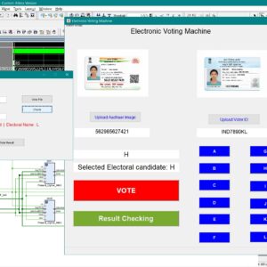
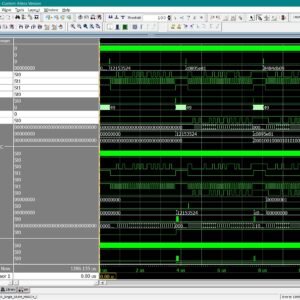
An Aadhaar-Authenticated FPGA-Based Electronic Voting Machine with EPIC Key Derived
Base paper Abstract:
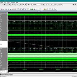
Electronic voting machines are widely used to improve election transparency, reduce manual effort, and provide faster result declaration when compared to traditional paper-based voting systems. The integration of digital platforms further enables ease of access, efficient data handling, and automated vote counting. However, existing electronic voting solutions still face critical challenges such as voter impersonation, data tampering, weak software-based security, and lack of strong hardware-level protection, especially when sensitive voter identity information is involved. Most current systems rely on microcontroller-based architectures, centralized databases, or conventional cryptographic algorithms, which introduce vulnerabilities related to key management, higher computational cost, and limited resistance to physical and logical attacks. To address these issues, this work proposes an Aadhaar-authenticated FPGA-based electronic voting machine with EPIC key–derived lightweight cryptographic vote protection. In the proposed system, Aadhaar number and Voter ID (EPIC) information are captured through a MATLAB-based graphical user interface and securely stored as voter records. The EPIC number is used to derive an 80-bit cryptographic key, while the complete voter information is formatted into a 256-bit data frame and processed within FPGA block memory. Lightweight PRESENT cipher encryption, along with cipher and key shuffling techniques, is employed to protect voter data at the hardware level, ensuring confidentiality and integrity. Decryption is performed using a reverse process to enable authenticated vote verification and result checking without exposing encrypted data. The novelty of this work lies in EPIC key–based dynamic key generation combined with FPGA-based lightweight cryptography, eliminating external key storage and reducing attack surfaces. The system ensures secure authentication, tamper resistance, low resource utilization, and reliable vote verification. Performance and functionality are validated using MATLAB for GUI and data handling, and Verilog HDL for FPGA implementation, demonstrating a secure, efficient, and hardware-trusted electronic voting solution.
List of the following materials will be included with the Downloaded Backup:FPGA IP Core for DC Motor Control with Adaptive Neural Network PID Tuning
Base paper Abstract:
Traditional proportional integral derivative (PID) falls short for precise control of DC motor speed under changing conditions. This paper presents a novel FPGA based IP (intellectual property) core for real-time PID parameter adjustment utilizing a multilayer neural network and the back propagation neural network algorithm. The design is implemented entirely in verilog HDL (hardware description language) using the Vivado 2023.1 tool in the Zynq 7z020 SoC (system on chip), with highly efficient resource utilization of 7.37% look-up table (LUT), 1.92% flip-flops, and 3.57% memory. The co-simulation results show a fast rise time of 0.00496s, a settling time of 0.0083s, a lower integral absolute error (IAE) of 0.045, and a minimum overshoot of 0.45%, validating the effectiveness of the proposed controller for comprehensive motion control systems. This dynamic approach outperforms traditional PID controllers by adapting to changing conditions, significantly improving rise time and settling time, which are critical factors in healthcare applications. Other key features of this work include precise duty cycle generation at a 10 kHz switching frequency for accurate motor speed control and an incremental encoder interface for high-resolution position feedback.
List of the following materials will be included with the Downloaded Backup:Design and analysis of Reversible Approximate Full Adder and its applications with Optimized 4:2, 5:2, 7:2 Compressors for Efficient Approximate Multipliers
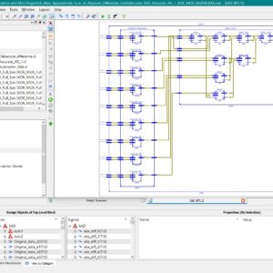
An Efficient Approximate Sum of Absolute Differences Hardware for FPGAs
Proposed Abstract:
Sum of Absolute Differences (SAD) is mainly applied in block-matching tasks such as motion estimation for video compression, stereo matching for depth/disparity calculation, template matching in image/object detection, image registration (including medical imaging), and lightweight optical-flow/tracking systems, because it is simple, fast, and hardware-friendly. The Traditional accurate SAD hardware provides exact results but consumes high power and requires large area, while existing approximate designs reduce cost but often suffer from high errors and poor FPGA-specific optimization. To overcome these limitations, this work proposes an improved SAD hardware architecture that replaces the conventional full adder with a lightweight XOR–MUX structure. This change reduces delay, minimizes area, and increases speed by removing redundant logic and optimizing FPGA resource utilization. The novelty of the design lies in combining approximation with FPGA-aware optimization, achieving bounded error, reduced power consumption, and higher operating frequency. The proposed system is implemented in Verilog HDL and tested on a Xilinx FPGA, showing improvements in LUT usage, clock frequency, and power efficiency, making it suitable for real-time video and image processing applications.
List of the following materials will be included with the Downloaded Backup:Scalable JTAG-Based 32-Bit Memory Test Architecture with MATS+ and MATS++/March-C Fault Detection
Proposed Abstract:
Embedded memories are increasingly used in advanced System-on-Chip (SoC) designs for applications such as networking, automotive control, and medical imaging, where reliability and performance are critical. Ensuring fault-free operation of these memories is essential, yet memory testing remains a major challenge. Conventional MBIST architectures, while effective, often introduce significant silicon overhead, add design complexity, and lack flexibility for post-fabrication updates. In addition, existing memory test algorithms have their own drawbacks: March-C is widely applied and provides high fault coverage, but it requires long test times due to bit-oriented operations and large numbers of read–write cycles; MATS+ is simple and efficient but suffers from lower coverage, particularly for coupling and complex dynamic faults; and MATS++ improves on MATS+ with better detection capability, yet it still trades off hardware cost and scalability when applied to larger 32-bit word-oriented memories. Furthermore, most existing implementations are optimized for small SRAMs and are not easily scalable to clustered embedded memories in SoCs, nor do they fully exploit standard boundary-scan infrastructure for low-cost testing. To address these problems, this work proposes a scalable JTAG-based 32-bit memory test architecture that reuses IEEE 1149.1 boundary-scan resources to apply and compare March-C, MATS+, and MATS++ algorithms in both single-bit and multi-bit test modes. The proposed framework minimizes additional hardware cost by integrating BIST control into boundary-scan registers, while enabling algorithm programmability and flexibility for different memory clusters. The novelty lies in providing a detailed performance comparison of these algorithms under a unified boundary-scan-based architecture, focusing on trade-offs between fault coverage, test time, and silicon overhead. The design is implemented in Verilog HDL and synthesized on an FPGA using Xilinx Vivado, where parameters such as area, power, and latency are evaluated to validate efficiency and practical applicability for SoC-level memory testing.
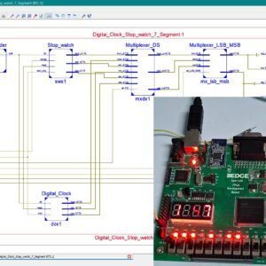
List of the following materials will be included with the Downloaded Backup:Design and Implementation of a Unified Digital Clock and Stopwatch System Using FSM and Multiplexed Seven-Segment Display
Proposed Abstract:
Digital clocks and stopwatches are widely used in daily applications such as consumer electronics, embedded devices, portable medical instruments, and time monitoring systems, as they provide simple and accurate time tracking functions. These systems offer advantages like low cost, user-friendly operation, and high reliability; however, they often face disadvantages such as hardware redundancy, higher power consumption, and limited integration when clock and stopwatch functions are implemented separately. The main problem addressed in this work is the lack of a unified architecture that can perform both digital clock and stopwatch operations using shared resources, which leads to inefficient hardware utilization and increased complexity in existing designs. Conventional systems generally use independent controllers and dedicated display drivers, resulting in additional overhead. To overcome this limitation, we propose a finite state machine based architecture that integrates both digital clock and stopwatch modules into a single design with common display hardware. The system employs multiplexers and control signals to switch seamlessly between clock and stopwatch modes, while states such as idle, hour, minute, second, and pause are clearly managed through FSM logic. The novelty of this work lies in the resource-sharing approach where a common seven-segment display is driven by multiplexed outputs, thereby reducing area, power, and switching complexity without compromising accuracy. The proposed design is implemented and tested using hardware description language coding and simulated on FPGA-based platforms, ensuring precise timing, functional correctness, and display reliability. Performance evaluation confirms that the system achieves efficient utilization of logic resources, accurate real-time operation, and flexibility for future extension in low-power VLSI and IoT-based applications.
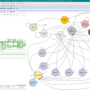
List of the following materials will be included with the Downloaded Backup:FPGA Implementation of Intelligent Elevator System for AI Applications
Proposed Abstract:
Intelligent elevator systems are used in many smart buildings, offices, hospitals, and tall apartments to move people quickly, reduce waiting time, and save energy. They have many advantages, like faster operation, better safety, and the ability to handle requests from many floors at the same time. But there are also some disadvantages, such as slow response when many people use them, fixed movement patterns that cannot adjust to real-time needs, weak security for restricted floors, and no use of advanced AI features for learning and prediction. Most existing elevator systems are built using microcontrollers with fixed scheduling methods, which cannot easily change their operation or add smart features. The problem in this work is to create an elevator system that works faster, is more secure, can adjust to different situations, and is ready for AI use, while also keeping passengers safe. In this project, we design an elevator controller on FPGA using a finite state machine. The system includes floor request handling, priority scheduling, emergency stop, overload detection, automatic door timing, floor number display, passcode access for special floors, and a fire alarm mode. The new idea in this work is to use the speed and flexibility of FPGA hardware along with an FSM design that can later connect to AI for learning passenger habits and predicting movement needs. This makes the system quick, safe, and adaptable. The design is written in Verilog HDL, tested in ModelSim, and implemented on a Xilinx FPGA board. We measure performance by checking response time, scheduling efficiency, and safety accuracy, and the results show it is suitable for future smart building use.
List of the following materials will be included with the Downloaded Backup:Resource and Energy Efficient Implementation of ECG Classifier using Binarized CNN for Edge AI Devices
Base Paper Abstract:
Wearable Artificial Intelligence-of-Things (AIoT) devices demand smart gadgets that are both resource and energy-efficient. In this paper, we explore efficient implementation of binary convolutional neural network employing function merging and block reuse techniques. The hardware implemented in field programmable gate array (FPGA) platform can classify ventricular beat in electrocardiogram achieving accuracy of 97.5%, sensitivity of 85.7%, specificity of 99.0%, precision of 92.3%, and F1-score of 88.9% while consuming only 10.5-µW of dynamic power dissipation.
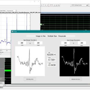
List of the following materials will be included with the Downloaded Backup:A Dual-Mode ECG Segment Export Tool with RGB and Grayscale Hex Encoding in MATLAB
Project Details :
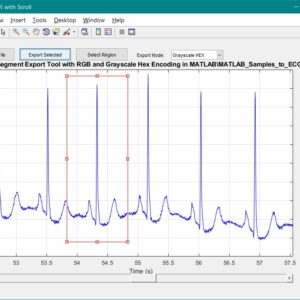
Electrocardiography (ECG) is a vital non-invasive diagnostic technique used to record the electrical activity of the heart. With increasing emphasis on digital healthcare and remote diagnostics, automated and efficient ECG data handling systems are becoming crucial. This work presents a MATLAB-based Graphical User Interface (GUI) framework designed for interactive ECG waveform analysis, segment selection, image generation, and hexadecimal encoding. The system accepts standard ECG data files in .txt format, processes them for visual inspection, and provides an intuitive scrollable interface to examine long-duration signals. A region of interest can be manually selected using a resizable rectangle tool. Upon selection, the user can export the waveform as a clean image (without axis ticks, titles, or grid lines) in a standardized resolution of 256×256 pixels. To accommodate further integration with embedded systems, AI pipelines, or hardware implementations, the application allows users to convert the exported image into either grayscale or RGB hexadecimal representations. The system supports two modes: RGB HEX (outputs R.txt, G.txt, B.txt) and Grayscale HEX (outputs Grayscale.txt), where each pixel’s intensity is encoded in two-digit hexadecimal format. This dual-format capability is controlled via a dropdown menu for easy toggling. The GUI is fully compatible with MATLAB R2018a and includes legacy support by replacing newer functions (such as writematrix) with older equivalents like dlmwrite. The application provides a real-time, interactive ECG visualization platform while also serving as a data preparation tool for machine learning models, microcontroller visualization, and FPGA-based healthcare signal processing. Its ability to convert waveform data into structured visual and hexadecimal forms bridges the gap between clinical signal acquisition and computational processing. This flexible, open-ended tool is particularly beneficial for researchers working in biomedical signal processing, embedded systems, and AI-based ECG classification.
List of the following materials will be included with the Downloaded Backup:Image Encryption on FPGA Using Chaotic PRNG and LFSR: TFT Display Integration
Proposed Abstract:
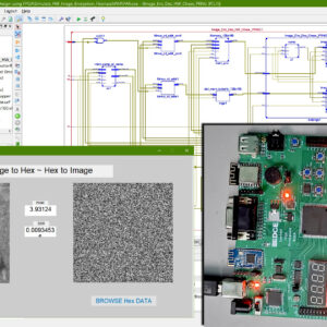
Image encryption plays a crucial role in securing digital communication, especially with the rise of cyber threats and data breaches. This research focuses on implementing a Chaos-based Pseudorandom Number Generator (PRNG) for image encryption and compares its performance with Fibonacci and Galois-based Linear Feedback Shift Registers (LFSRs). The proposed system is developed using Verilog HDL and synthesized on a Xilinx Spartan-6 FPGA, with a real-time TFT display interface for encrypted and decrypted image visualization. Traditional LFSR-based PRNGs are widely used due to their simplicity and speed; however, they suffer from predictable periodicity and lower security strength. In contrast, Chaos-based PRNGs provide higher randomness and security, making them ideal for cryptographic applications. In this work, different PRNG approaches are analyzed based on randomness quality using the NIST test suite, hardware resource utilization (LUTs, FFs, power consumption), and encryption security (correlation, entropy, and key sensitivity). The Chaos-based PRNG is then integrated into a stream cipher encryption system, where image pixels are transformed using bitwise XOR and chaotic substitution-permutation operations. The encrypted images are decrypted using the inverse transformation and displayed on a TFT display, ensuring real-time validation. Experimental results confirm that the Chaos-based PRNG outperforms LFSR-based PRNGs in security strength and randomness, while maintaining efficient FPGA resource utilization. This work demonstrates a practical hardware-based image encryption system, suitable for real-time, secure multimedia applications such as IoT, medical imaging, and defense systems. Future enhancements include optimizing chaos-based PRNGs for high-speed cryptographic applications and exploring AI-based encryption techniques for enhanced security.
List of the following materials will be included with the Downloaded Backup:Low voltage high speed 8T SRAM cell for ultra-low power applications
Proposed Abstract:
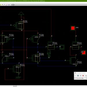
The usage of portable devices increasing rapidly in the modern life has led us to focus our attention to increase the performance of the SRAM circuits, especially for low power applications. Basically in Six-Transistor (6T) SRAM cell either read or write operation can be performed at a time whereas, in 7T SRAM cell using single ended write operation and single ended read operation both write and read operations will be accomplished simultaneously at a time respectively. When it comes to operate in sub threshold region, single ended read operation will be degraded severely and single ended write operation will be severely degraded in terms of write-ability at lower voltages. To encounter these complications, an eight transistor SRAM cell is proposed. It performs single ended read operation and single ended write operation together even at sub threshold region down to 0.1V with improved read-ability using read assist and improved dynamic write-ability which helps in reducing the consumption of power by attaining a lower data retention voltage point. To reduce the total power consumption in the circuits, two extra access transistors are used in 8T SRAM cell which also helps in reducing the overall delay.
List of the following materials will be included with the Downloaded Backup:FPGA Implementation of a ECG-DAC-SPI Interface for Medical Applications
Proposed Abstract:
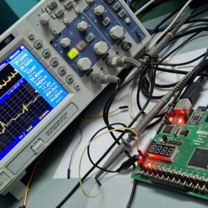
This project presents the design and implementation of an ECG-DAC-SPI interface for medical applications using the Xilinx Spartan-6 FPGA platform and the MCP4921 12-bit SPI DAC. The objective is to process pre-recorded ECG signals from the MIT-BIH database, reconstruct the signal digitally, and output it as an accurate analog waveform suitable for real-time monitoring and simulation. The system is designed to meet the stringent requirements of medical-grade signal fidelity and low-latency processing. The FPGA-based implementation comprises several key modules, including digital ECG data acquisition, optional noise filtering, and a custom SPI communication controller. The ECG signal, preloaded into FPGA memory, is scaled and quantized to match the 12-bit resolution of the MCP4921 DAC. A low-pass FIR filter is implemented on the FPGA to enhance signal quality by removing high-frequency noise, ensuring smooth signal. A Verilog HDL-based SPI controller facilitates precise communication with the DAC, synchronizing data transfer and ensuring real-time signal conversion. The reconstructed analog ECG waveform is visualized on an oscilloscope to validate its fidelity to the original dataset. The DAC, interfaced via the FPGA’s SPI controller, is chosen for its high resolution and compatibility with low-latency applications. The design is synthesized, implemented, and tested on the Xilinx Spartan-6 FPGA platform. The project includes extensive simulation and hardware testing, evaluating parameters such as SPI throughput, waveform accuracy, and system latency. Results demonstrate that the system achieves precise signal reconstruction and reliable analog output, suitable for medical applications. This work highlights the use of FPGA technology and the MCP4921 DAC for scalable and reconfigurable ECG signal processing systems. It provides a robust platform for integration into advanced medical devices, including real-time ECG monitors, simulators, and portable diagnostic tools. Future extensions of the design could include integration of live ECG sensors, advanced noise filtering, or wireless transmission for telemedicine applications.
List of the following materials will be included with the Downloaded Backup:Design and Implementation of Arithmetic Logic Unit in DSCH3 and Microwind
Proposed Abstract:
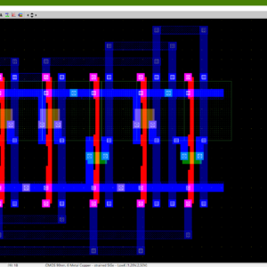
The Arithmetic Logic Unit (ALU) is a fundamental component in digital systems, particularly in the central processing units (CPUs) of microprocessors, where it executes essential arithmetic and logical functions. This paper presents the design and implementation of an 8-bit Arithmetic Logic Unit (ALU) using CMOS technology, developed and simulated in DSCH3 and Microwind environments. The primary goal of this research is to design an efficient and compact ALU optimized for performance and area efficiency. The 8-bit ALU performs eight operations: ripple carry addition, ripple borrow subtraction, multiplication, XOR, left shift, right shift, NAND, and NOR. Each logic gate within the ALU is constructed using CMOS logic to enhance power efficiency and integration density. This paper provides a detailed description of the ALU's CMOS-based architecture, its key components, and the control mechanism for operation selection. Performance metrics, including speed, area efficiency, and power consumption, are analyzed to assess the ALU’s effectiveness in CMOS technology.
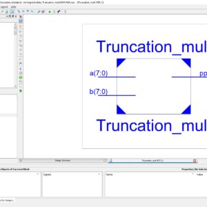
List of the following materials will be included with the Downloaded Backup:FPGA Implementation of 8×8 Truncated Multiplier Using Brent Kung Parallel Prefix Adder
Proposed Abstract:
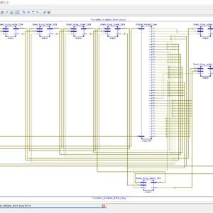
Multiplication is a critical operation in many digital signal processing and machine learning applications, where fast and efficient computation is essential. However, conventional multipliers that compute n x n bit products result in significant hardware overhead and increased power consumption. To address these challenges, this paper proposes an FPGA implementation of an 8x8 truncated multiplier utilizing the Brent-Kung parallel prefix adder to improve both speed and resource efficiency. The proposed truncated multiplier limits the output to n bits, discarding the least significant bits and utilizing a variable correction technique to minimize the error introduced by truncation. By selectively summing the most significant columns, the design achieves a balance between accuracy and hardware efficiency, providing a reduced-area solution for approximate computing. The Brent-Kung parallel prefix adder is integrated into the multiplier architecture to optimize the carry propagation stage, reducing the overall critical path delay. This adder is known for its logarithmic depth, which significantly improves the speed of the summation process while using fewer logic gates compared to traditional adders. This design was implemented in Verilog HDL and synthesized on a Xilinx Virtex-5 FPGA platform. Comparative analysis with a conventional multiplier shows that the proposed truncated multiplier achieves a notable reduction in FPGA resource utilization, including logic elements and power consumption, without sacrificing significant accuracy. The architecture particularly suitable for applications where speed and low power consumption are paramount, such as real-time image processing, DSP systems, and machine learning accelerators.
List of the following materials will be included with the Downloaded Backup:FPGA Implementation of Comparative Analysis and Performance Evaluation for Different LFSR Techniques
Proposed Abstract:
In this study, we explore the implementation and performance evaluation of various Linear Feedback Shift Register (LFSR) techniques on Field Programmable Gate Arrays (FPGAs). LFSRs are fundamental components in numerous digital applications, including cryptography, pseudorandom number generation, error detection, and secure communications. We specifically focus on five different LFSR methodologies: Fibonacci LFSR, Galois LFSR, Non-Linear Feedback Shift Register (NLFSR), Modular LFSR and Masked LFSR. Each technique is implemented on an FPGA platform, utilizing Verilog HDL for design specification and synthesis. The study begins with a detailed examination of the theoretical underpinnings and operational mechanisms of each LFSR technique, followed by their FPGA implementations. We then conduct a comprehensive performance analysis, focusing on critical parameters such as area utilization, power consumption, throughput, and randomness quality. The analysis reveals the strengths and trade-offs associated with each method, providing insights into their suitability for various applications. Our results demonstrate that while Fibonacci and Galois LFSRs offer simplicity and ease of implementation, more advanced techniques like NLFSR and Masked LFSR provide enhanced security features at the cost of increased complexity. The study concludes with recommendations on selecting the appropriate LFSR technique based on the specific requirements of the application, highlighting the balance between security, performance, and resource efficiency in FPGA-based designs.
List of the following materials will be included with the Downloaded Backup:Ultra Lightweight Cryptography: Exploring the Application and Optimization of the PRESENT Cipher
Proposed Abstract:
The PRESENT cipher, an ultra-lightweight block cipher, has been designed specifically for environments where resource constraints are a critical factor, such as RFID tags, sensor networks, and various IoT devices. Its compact design, featuring a 64-bit block size, 80-bit key, and 31 rounds, makes it particularly suitable for applications requiring minimal hardware resources, low power consumption, and moderate security. Unlike more robust ciphers like AES, which demand significant computational and memory resources, PRESENT strikes an optimal balance between efficiency and security for constrained devices. This paper explores the practical applications of the PRESENT cipher in secure communication protocols, device authentication, and data encryption in low-power systems. By synthesizing 16-bit, 32-bit, and 64-bit implementations on a Xilinx Virtex-5 FPGA, we demonstrate the cipher’s adaptability across a range of use cases, analyzing key performance metrics such as area, delay, and power consumption. Our findings indicate that PRESENT is highly effective in scenarios where traditional cryptographic solutions are too resource-intensive, offering a viable alternative for securing data in pervasive computing environments. PRESENT’s applications extend to securing communication in embedded systems, protecting sensitive information in contactless payment systems, and enabling secure data transmission in wireless sensor networks. The cipher’s lightweight design ensures that it can be implemented in devices with limited processing capabilities, making it an ideal choice for modern IoT applications. However, the trade-off between security and efficiency must be carefully considered. While PRESENT is suitable for applications with moderate security requirements, it may not provide the level of protection needed for high-security environments.
List of the following materials will be included with the Downloaded Backup:Efficient Image Conversion and Restoration System with Hexadecimal Encoding and Quality Evaluation
Abstract:
The proposed work aims to facilitate the conversion of images into a hexadecimal format for efficient storage and manipulation, and subsequently restore them to their original form. This conversion is beneficial for reducing storage space and simplifying data transmission. The system supports multiple color spaces, including grayscale, RGB, and YCbCr, enhancing its versatility in image processing tasks. Users select an image file, which the system processes according to the selected mode: converting the image or its channels to a hexadecimal format and saving the data to files. During restoration, the system reads the hexadecimal files, reconstructs the image, and displays it. To ensure the fidelity of the restored images, the system computes and displays quality metrics such as Peak Signal-to-Noise Ratio (PSNR), Mean Squared Error (MSE), and Structural Similarity Index (SSIM). This comprehensive solution provides an efficient method for image data handling and quality assessment, ensuring accurate and reliable image restoration.
Proposed System:The proposed system aims to facilitate the conversion of images into a hexadecimal format and subsequently restore them to their original form. This system supports multiple color spaces, including grayscale, RGB, and YCbCr, and evaluates the quality of the restored images using metrics such as Peak Signal-to-Noise Ratio (PSNR), Mean Squared Error (MSE), and Structural Similarity Index (SSIM).
List of the following materials will be included with the Downloaded Backup:Implementation of High-Precision MFCC Feature Extraction Using FPGA for Speech Recognition
Proposed Abstract:
Speaker recognition is one of the technologies that may be used for biometric identification, and it offers higher application possibilities in many sectors. At the moment, the implementation of the speaker identification algorithm on the hardware is mostly dependent on the SOC of the FPGA. An FPGA-based real-time technique for extracting acoustic characteristics is presented in this research. The method is based on MFCC, which stands for Mel Frequency Cepstral Coefficients. The trials have shown that the FPGA-based MFCC calculation has a high level of accuracy; the purpose of this study is to enhance the performance assessment of MFCC by making use of novelty-based architecture. In this study, a technique for FPGA-based speech recognition is provided. This approach was developed by investigation and analysis of the speaker recognition algorithm. The IFFT, the Mell filter, the DFT, the derivatives, and the Hamming Window with pre-emphasis are every aspect of this approach. This proposed MFCC will be constructed with an AHB interface in order to facilitate higher access DMA Controller when it is used in SOC applications. This work was carried out using Verilog HDL, and it was generated with Xilinx Vivado FPGA. Additionally, all of the parameters were analyzed and compared with regard to area, latency, and power.
List of the following materials will be included with the Downloaded Backup:A Reversible Processor Architecture and Its Reversible Logic Design
Proposed Abstract:
This paper presents the design and FPGA implementation of a 16-bit reversible processor architecture employing Fredkin, Feynman, and PERES gate architectures for reversible logic design. Reversible computing offers promising advantages in terms of energy efficiency and information loss prevention, making it suitable for various emerging computing paradigms. The proposed processor architecture encompasses a carefully crafted instruction set, data path, and control logic, all realized using reversible logic gates. Key components such as the ALU, register file, and memory elements are designed with an emphasis on reversibility. The design is implemented using Hardware Description Languages (HDLs), targeting a specific FPGA platform. The paper outlines the design methodology, gate-level implementation details, memory design considerations, FPGA synthesis, and testing procedures. Furthermore, it discusses optimization strategies and presents simulation results to validate the functionality and efficiency of the proposed reversible processor architecture. This work contributes to the advancement of reversible computing and provides insights into the practical realization of reversible processor architectures on FPGA platforms.
List of the following materials will be included with the Downloaded Backup:FPGA Implementation of TFT 1.8 inch SPI 128×160 Display ROM Interface
Simple Description:
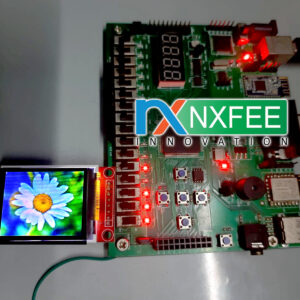
This ST7735R is a display controller used in small TFT (Thin-Film Transistor) LCD displays. It is often used in combination with microcontrollers or FPGAs to drive these displays. The controller supports the Serial Peripheral Interface mode of communication for sending commands and data to the display. This TFT display helps with a greater number of image and video processing applications. Here we have implemented this TFT display in FPGA hardware implementation using Verilog HDL with a novelty-based architecture design. Finally shown the output with TFT Display.
List of the following materials will be included with the Downloaded Backup:FPGA Implementation of Spread Spectrum Clock Generator with Onion Modulation
Proposed Abstract:
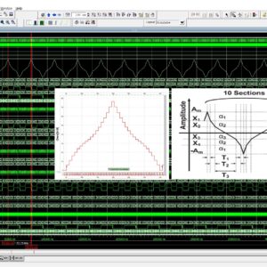
A Spread Spectrum Clock Generator (SSCG) is used in electronics to purposefully vary the frequency of a clock signal via modulation. Modulation is accomplished by dispersing the energy of the signal throughout a spectrum of frequencies rather than focusing it on a certain frequency. The main objective of using the spread spectrum approach in clock generation is to minimize electromagnetic interference (EMI) and enhance electromagnetic compatibility (EMC) in electronic systems. The main reason for using many layers of modulation in spread spectrum clock production, regardless of whether the name "Onion Modulation" is used, is to provide a more advanced and adaptable method for reducing electromagnetic interference. The primary design feature of the onion wave is that the core portion of the waveform has the least steep slope, which serves to generate the output. In order to optimize the frequency effect design, the conventional approach involves using a memory ROM to regulate the slope and obtain the desired onion waveform. This current methodology necessitates substantial memory allocation and an intricate architecture, resulting in higher power consumption. The proposed method presents a unique architecture for onion modulation, which offers reduced logic size and power usage. This architecture was created using Verilog HDL, tested using Modelsim, and implemented using the Xilinx Vertex-5 FPGA.
List of the following materials will be included with the Downloaded Backup:An Innovative Area Efficient Pixel Shuffling Method for Image Encryption Algorithm
Proposed Abstract:
In image processing and computer vision, pixel shuffling is a method used to increase an image's resolution without adding more parameters or network complexity. With this technique, a low-quality image's pixels are rearranged to produce an output with a better resolution. Pixel shuffling has proven successful in a number of applications, such as image synthesis, super-resolution, and style transfer. Its simplicity and efficiency make it an attractive option for tasks where increasing image resolution is essential, while avoiding the computational overhead associated with more complex architectures. The image line buffer based pixel shuffling technique presented in this study is an alternative to the classic method, which takes up more logic space in VLSI implementations. This proposed method splits and reconstructs the source photos using a 5x5 image line buffer. With the use of block interleave techniques, this pixel shuffling approach handled row and column sequence using this 5x5 picture line buffer. In conclusion, this study was compared with the PSNR and SSIM value; comparisons of logic sizes for area, latency, and power were also examined.
List of the following materials will be included with the Downloaded Backup:FPGA Implementation of 64 Block Data Encryption Standard Algorithm
Proposed Abstract:
The Data Encryption Standard (DES) is widely recognized as the inaugural and prevailing symmetric key method used for the cryptographic processes of encrypting and decrypting digital data. Despite its lack of security against determined attackers in contemporary times, the use of this method persists in older systems. This work introduces a novel implementation of the Data Encryption and Decryption Standard algorithm using Field Programming Gate Arrays (FPGAs) that prioritizes security, high throughput, and space efficiency. The suggested solution involves the creation of a system that utilizes a block size of 64 bits and a key length that is also 64 bits. Additionally, the system operates with a data width of 64 bits. This achievement is accomplished by integrating the notion of pipelining with time variable permutations, and then comparing it with previously shown encryption techniques. The permutations undergo temporal variations under the control of the cryptographer. Hence, the cipher text also undergoes alteration while the key and plaintext remain constant. The algorithm under consideration has been successfully executed on the Xilinx Vetex-5 Field-Programmable Gate Array (FPGA) platform. The findings of this study indicate that the suggested implementation exhibits exceptional speed in comparison to other hardware implementations. Additionally, it demonstrates superior area efficiency and significantly enhanced security measures.
List of the following materials will be included with the Downloaded Backup:FPGA Implementation of Image Line Buffer to Split and reconstruct a 3×3 size of image pixel with using FIFO Design
Proposed Abstract:
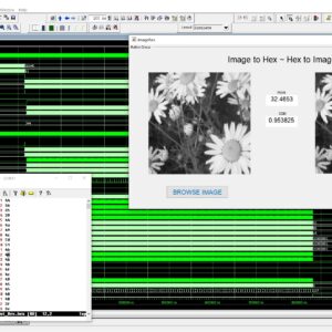
Image line buffers are used in several kinds of image processing applications, particularly where operations must be executed on a per-line basis in order to optimize efficiency. There are many typical applications associated with this technology, including real-time video processing, image filtering, edge detection, computer vision, memory optimization, parallel processing, compression algorithms, and medical imaging. In the context of image and video processing applications, the use of image line buffers may contribute to the optimization of operations when dealing with a continuous stream of frames processed in real time. In the context of image processing, convolutional processes are often used for tasks like as image filtering and blurring. These operations are typically carried out on a per-pixel basis, wherein the value assigned to each pixel is determined by the values of its adjacent pixels. The proposed structure was created using a First-In-First-Out (FIFO) based approach, aiming to decrease the number of logic sizes and complexity in Very Large Scale Integration (VLSI) design architecture. The conversion of design images to hexadecimal and hexadecimal to image format is accomplished using MATLAB GUI applications. These applications also facilitate the comparison of Peak Signal-to-Noise Ratio (PSNR) and Structural Similarity Index Measure (SSIM) values. The internal architecture of the system is implemented using Verilog Hardware Description Language (HDL). Additionally, the simulation is conducted using Modelsim. Furthermore, the system's performance parameters, including area, delay, and power consumption, are compared with those of the Xilinx Vertex-5 Field Programmable Gate Array (FPGA).
List of the following materials will be included with the Downloaded Backup:Smart Intelligent and Adaptive Traffic Controller using FPGA
Proposed Abstract:
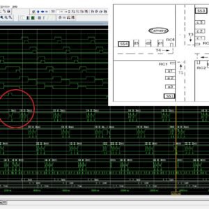
Traffic management is a critical aspect of modern urban infrastructure, and the ever-increasing volume of vehicles on the road demands innovative and adaptive solutions. This work presents a novel approach to traffic control using Field-Programmable Gate Arrays (FPGAs) as the core technology. The proposed system leverages the capabilities of FPGAs to create a Smart, Intelligent, and Adaptive Traffic Controller that can revolutionize urban traffic management. One of the key features of the proposed work is its adaptability. The system can dynamically adjust traffic signal timings and lane allocations in response to changing traffic patterns of 4-way road conditions with the help of sensor inputs. This methodology adaptability enhances road safety and minimizes traffic delays. The use of FPGA technology in the Traffic controller provides several advantages, including high computational performance, low power consumption, and the ability to reconfigure the system as traffic management needs evolve. Additionally, the system is highly scalable and can be deployed in various urban settings.
List of the following materials will be included with the Downloaded Backup:Design and Implementation of Arithmetic Logic Unit in HDL
Proposed Abstract:
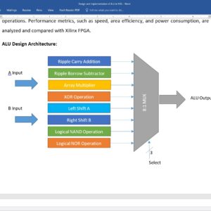
Arithmetic logic unit (ALU) is an important part of all digital gadgets and applications. This paper presents the design and implementation of an 8-bit Arithmetic Logic Unit (ALU) with a capability to perform eight distinct operations. ALUs are fundamental components in the central processing units (CPUs) of microprocessors and are responsible for executing arithmetic and logical operations. The primary objective of this research is to design an efficient and versatile 8-bit ALU that can execute a wide range of operations while optimizing for performance and area efficiency. The proposed 8-bit ALU is designed to perform the following eight operations: Ripple carry addition, Ripple borrow subtraction, Array multiplication, XOR operation, left shift, right shift, NAND operation and a logical NOR operation. The research presents a detailed description of the ALU's architecture, its constituent components, and the control mechanism for selecting operations. Performance metrics, such as speed, area efficiency, and power consumption, are analyzed and compared with Xilinx FPGA.
List of the following materials will be included with the Downloaded Backup:Efficient Design of Behavioral Clock Divider for Multiple Frequency
Proposed Abstract:
Frequency dividers are of utmost importance in frequency synthesizers that are based on phase locked loops. The use of dual modulus presales enhances the versatility of the design in both integer and Fractional-N frequency synthesizers. The selection of an acceptable division ratio is dependent upon the channel spacing and frequency range of the synthesizer. There are several techniques for division in electronic systems, including the injection locked frequency divider (ILFD), complementary ILFDs, flip flop based dividers, dual modulus dividers, and modular dividers. Therefore, these approaches possess some advantages and disadvantages, such as reduced jitter, a restricted frequency tuning range, increased circuit size due to the addition of an LC tank circuit, increased power consumption, and lower quality factor. This work aims at addressing certain issues pertaining to clock dividers and proposes a unique design that utilizes a multiple digital frequency divider based on D flip flops. The architectural design is predicated on the use of a phase shifting mechanism using a D flip flop, which effectively controls the division ratio. The present study involves the use of a preliminary phase shifting melody in conjunction with the Digital Clock Manager (DCM). The auto tuning strategy described in this study aims to adjust the phase difference between two differential clock signals. By intentionally inducing metastability in one or more flip flops, the proposed approach utilizes a digital clock manager in a clock divider to mitigate the effects of metastability and reduce jitter across multiple tuning frequencies. Furthermore, it is worth noting that the logic size and power consumption required for its operation are significantly reduced.
List of the following materials will be included with the Downloaded Backup:Design of Approximate Restoring Divider
Proposed Abstract:
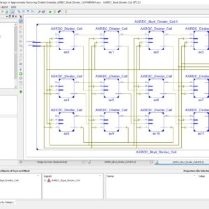
Approximate computing is an emerging paradigm in error-tolerant applications that leads to power-efficient designs without significant loss in quality. The divider in these applications have complex hardware and more latency among the computational blocks resulting in power consumption. Hence approximating the division module would lead to designs with vastly improved power efficiency. A new approximate subtractor (AxSUB) is proposed in this paper with the intent to reduce the hardware complexity while achieving accuracy within permissible limits. The proposed AxSUB and existing approximate subtractor units are used in the restoring array division (RAD) architecture to prove the efficacy of the AxSUB. This proposed architecture design with 8/4 approximate divider using Verilog HDL and synthesized using Xilinx Spartan 6 FPGA, and proved the performance of area, delay and power.
List of the following materials will be included with the Downloaded Backup:Hamming based Single Fault Error Correction Code
Proposed Abstract:
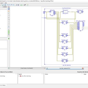
Signal processing and communication systems often use digital filters. In certain circumstances, the dependability of such systems is essential, prompting the construction of fault-tolerant filters. Many methods that take use of the structure and characteristics of the filters to achieve fault tolerance have been put forward throughout the years. Technology advances permit more intricate systems with several filters. It is typical for some of the filters in such complicated systems to function in simultaneously, for instance by using the same filter on several input signals. Recently, a straightforward method for achieving fault tolerance was given that takes use of the existence of parallel filters. This paper expands on that concept to demonstrate how error correction codes (ECCs), in which each filter is the equivalent of a bit in a conventional ECC, may be used to secure parallel filters. When there are several parallel filters operating simultaneously, this new technique enables more effective protection. The efficiency of the method in terms of protection and implementation cost is assessed using a case study of parallel finite impulse response filters.
List of the following materials will be included with the Downloaded Backup:FPGA Implementation of High Performance Reversible logic based 16×16 Array Multiplier
Proposed Abstract:
In this recent technology of digital gadgets and digital signal processing and image processing method will have more priority in arithmetic operation, such as multiplication, divisions, addition and subtractions. In this operations of arithmetic unit will have number of garbage signal with more memory logic element, due to this problem these arithmetic operations will take more area, delay and power in VLSI system design. Here, this proposed work will present a arithmetic operation using reversible logic method, thus it take memory less logic and less garbage elements, therefore here this reversible logic method will integrated using reversible half adders and full adder in array multiplier and proved the performance with less garbage signals. Finally, this work will have integrated in Verilog HDL, simulated in Modelsim and Synthesized in Xilinx FPGA, and also compared all the parameter in terms of area, delay and power.
List of the following materials will be included with the Downloaded Backup:FPGA Implementation of 8×8 Truncated Multiplier
Proposed Abstract:
The operation of multiplication is an often encountered need in the field of digital signal processing. Parallel multipliers provide a rapid approach for performing multiplication operations, while demanding a significant amount of space in VLSI (Very Large Scale Integration) implementations. In the majority of signal processing applications, there is a preference for using a rounded result in order to prevent an increase in the size of the word. Therefore, an important goal in the design process is to minimize the spatial demand of the rounded output multiplier. This study introduces a novel approach to parallel multiplication that efficiently calculates the products of two n-bit values by selectively summing the most important columns using a variable correction technique. This research furthermore includes a comparative analysis of the implementation of 8X8 conventional and truncated multipliers using Verilog Hardware Description Language (HDL) on Field Programmable Gate Arrays (FPGAs). The shortened multiplier demonstrates a much greater decrease in device consumption as compared to the regular multiplier. A conventional multiplier performs computations on n x n bits and produces a weighted sum of the output, consisting of 2n bits. In contrast, a truncated multiplier generates an output of just n bits from the n x n bit input. The use of logic gates in both internal and external hardware design will be decreased. Truncated multipliers provide a viable approach for achieving significant reductions in FPGA resources, latency, and power consumption compared to regular parallel multipliers, particularly in scenarios where the complete accuracy provided by the standard multiplier is unnecessary.
List of the following materials will be included with the Downloaded Backup:Provide Wordlwide Online Support
We can provide Online Support Wordlwide, with proper execution, explanation and additionally provide explanation video file for execution and explanations.
24/7 Support Center
NXFEE, will Provide on 24x7 Online Support, You can call or text at +91 9789443203, or email us nxfee.innovation@gmail.com
Terms & Conditions:
Customer are advice to watch the project video file output, and before the payment to test the requirement, correction will be applicable.
After payment, if any correction in the Project is accepted, but requirement changes is applicable with updated charges based upon the requirement.
After payment the student having doubts, correction, software error, hardware errors, coding doubts are accepted.
Online support will not be given more than 3 times.
On first time explanation we can provide completely with video file support, other 2 we can provide doubt clarifications only.
If any Issue on Software license / System Error we can support and rectify that within end of day.
Extra Charges For duplicate bill copy. Bill must be paid in full, No part payment will be accepted.
After payment, to must send the payment receipt to our email id.
Powered by NXFEE INNOVATION, Pondicherry.
Call us today at : +91 9789443203 or Email us at nxfee.innovation@gmail.com
NXFEE Development & Services

Product Categories
- 2014 (11)
- 2015 (39)
- 2016 (30)
- 2017 (16)
- 2018 (17)
- 2019 (42)
- 2020 (29)
- 2021 (17)
- 2022 (23)
- Accessories (47)
- Area Efficient (117)
- High speed VLSI Design (57)
- IEEE (15)
- Image Processing (40)
- Low power VLSI Design (99)
- NOC VLSI Design (2)
- VLSI (253)
- VLSI 2023 (21)
- VLSI 2024 (18)
- VLSI 2025 (33)
- VLSI 2026 (4)
- VLSI Application / Interface and Mini Projects (31)
- VLSI_2023 (15)
Filter by price
Product Status
Sort by producents

Copyright © 2026 Nxfee Innovation.

