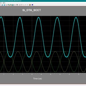
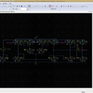
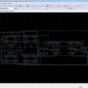
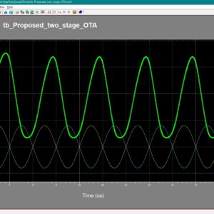
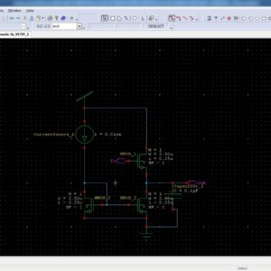
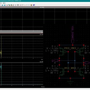
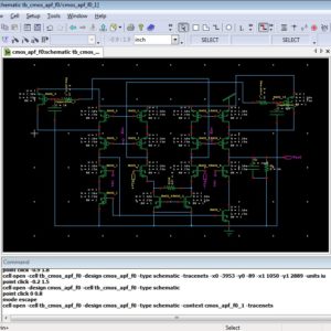
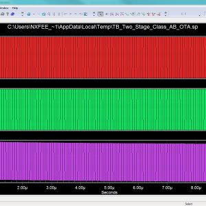
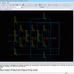
0.4-V nW-Power High-Gain Bulk-Driven Two-Stage OTA With Self-Cascode Composite Transistors
Implementation techniques and results for a recently proposed real-time reconfigurable low-pass equalizer (RLPE) consisting of a variable bandwidth (VBW) filter and a variable equalizer (VE) are presented. Both components utilize fixed finite-length impulse response (FIR) filters combined with a few general multipliers, resulting in lower area and power consumption compared to a general FIR filter, despite requiring more multiplications. This is because the constant multipliers in the fixed FIR filters of the RLPE can be optimized for implementation. An additional advantage is that the proposed RLPE does not require online design. Various implementation alternatives for fixed FIR filters, including ways to increase the frequency, are evaluated to optimize the implementation of the RLPE. Several versions of the proposed RLPE and a general FIR filter for comparison are implemented using a 28-nm fully depleted silicon on insulator (FD-SOI) standard cell library. The results demonstrate that the RLPE baseline design requires less power and area than the general equalizer, and although the frequency of the baseline implementation is lower, the design can reach the same frequency while still having significantly less power and area. Furthermore, an approach is introduced to break the chain in the polynomial section of the VBW filter by using fewer additional registers compared to standard pipelining. Instead, this method reformulates the constant multiplication problem to produce correct results. For the considered case, the power consumption is reduced between 49% and 70% for different frequencies, with an area decrease in the range of 64% to 67%, by using the proposed RLPE compared to a general FIR filter. Index Terms: Constant multiplications, real-time reconfiguration, variable bandwidth (VBW) low-pass filter, variable equalizer (VE).
List of the following materials will be included with the Downloaded Backup:40-Gb/s 0.7-V 2:1 MUX and 1:2 DEMUX with Transformer-Coupled Technique for SerDes Interface
This paper explores the use of transformer-coupled (TC) technique for the 2:1 MUX and the 1:2 DEMUX to serialize-and-deserialize (SerDes) high-speed data sequence. The widely used current-mode logic (CML) designs of latch and multiplexer/demultiplexer (MUX/DEMUX) are replaced by the proposed TC approach to allow the more headroom and to lower the power consumption. Through the stacked transformer, the input clock pulls down the differential source voltage of the TC latch and the TC multiplexer core while alternating between the two-phase operations. With the enhanced drain-source voltage, the TC design attracts more drain current with less width-to-length ratio of NMOS than that of the CML counterpart. The source-offset voltage is decreased so that the supply voltage can be reduced. The lower supply voltage improves the power consumption and facilitates the integration with low voltage supply SerDes interface. The MUX and the DEMUX chips are fabricated in 65-nm standard CMOS process and operate at 0.7-V supply voltage. The chips are measured up to 40-Gb/s with sub-hundred milliwatts power consumption.
List of the following materials will be included with the Downloaded Backup:
A 0.3-V 37-nW 53-dB SNDR Asynchronous Delta–Sigma Modulator in 0.18-μm CMOS
Abstract:
A new solution for an ultralow-voltage bulk driven (BD) asynchronous delta–sigma modulator is described in this paper. While implemented in a standard 0.18-µm CMOS process from the Taiwan Semiconductor Manufacturing Company and supplied with VDD = 0.3 V, the circuit offers a 53.3-dB signal-to-noise and distortion ratio, which corresponds to 8.56-bit resolution. In addition, the total power consumption is 37 nW, the signal bandwidth is 62 Hz, and the resulting power efficiency is 0.79 pJ/conversion. The above-mentioned features have been achieved employing a highly linear transconductor and a hysteretic comparator based on nontailed BD differential pair.
List of the following materials will be included with the Downloaded Backup:A 13.4-MHz Relaxation Oscillator With Temperature Compensation
Abstract:
A low-phase-noise relaxation oscillator uses a digital compensation loop to reduce its temperature coefficient (TC). This relaxation oscillator is fabricated in the 0.18-µm CMOS process. The measured average oscillation frequency is 13.4 MHz. The whole oscillator consumes 157.8 µW under a 1.2-V supply. The measured average TCs of the oscillation frequency with and without compensation are 193.15 and 1098.7 ppm/◦C, respectively. The TC achieves an improvement of 5.7 times. The measured frequency variation is within ±2% from −20 ◦C to 100 ◦C by using the digital compensation loop. The measured phase noise at 100-kHz offset frequency is −104.82 dBc/Hz, and the measured figure of merit (FOM) is −154.4 dBc/Hz
List of the following materials will be included with the Downloaded Backup:A 16-bit 2.0-ps Resolution Two-Step TDC in 0.18-μm CMOS Utilizing Pulse-Shrinking Fine Stage
Abstract:
This paper proposes a time-to-digital converter (TDC) that achieves wide input range and fine time resolution at the same time. The proposed TDC utilizes pulse-shrinking (PS) scheme in the second stage for a fine resolution and two-step (TS) architecture for a wide range. The proposed PS TDC prevents an undesirable non-uniform shrinking rate issue in the conventional PS TDCs by utilizing a built-in offset pulse and an offset pulse width detection schemes. With several techniques, including a built-in coarse gain calibration mechanism, the proposed TS architecture overcomes a nonlinearity due to the signal propagation and gain mismatch between coarse and fine stages. The simulation results of the TDC implemented in a 0.18-µm standard CMOS technology demonstrate 2.0-ps resolution and 16-bit range that corresponds to ∼130-ns input time interval with 0.08-mm2 area. It operates at 3.3 MS/s with 18.0 mW from 1.8-V supply and achieves 1.44-ps single-shot precision. Index Terms— Built-in calibration, pulse shrinking (PS), time-to-digital conversion, two step (TS).
List of the following materials will be included with the Downloaded Backup:A 2.5-V 8-Bit Low power SAR ADC using POLC and SMTCMOS D-FF for IoT Applications
Abstract:
A 2.5-V 8-bit low force and efficient Successive Approximation Register Analog-to-Digital converter (SAR-ADC) utilizing a Principled Open Loop Comparator (POLC) and Switched Multi-Threshold Complementary Metal Oxide Semiconductor (SMTCMOS) D-FF shift Register. In light of high proficiency and low force applications SAR-ADC is increasingly well known, yet it experience the ill effects of resolution and speed confinements. To defeat the above issue proposed a systematic methodology uses low force POLC based SAR-ADC is structured. Considering about the resolution, speed and compact design of 8- bit SAR-ADC, the proposed POLC strategy reasonably diminishes the propagation delay by 37% and decreases the force utilization by 62% appeared differently in relation to the standard system. A D-flip flop is planned to employ SMTCMOS procedure which has low force utilization and productively decline the leakage power. All the above circuits are simulated by using TANNER-EDA tool in 0.25μm CMOS technology produces 97% Efficiency.
List of the following materials will be included with the Downloaded Backup:A 25-Mb/s 4-ASK Receiver Front-End in 65-nm CMOS for Biomedical Data Telemetry via a Capacitive Link
This brief presents a 25-Mbps 4-amplitude-shiftkeying (4-ASK) receiver front-end (RFE) for biomedical data telemetry via a series-resonant capacitive link. The RFE incorporates low-power clock and data recovery (CDR) circuitry for synchronization in which a novel highly linear trans conductance (Gm) cell is employed in the phase detector (PD) to mitigate any possible error decisions while comparing the phase difference between the input and feedback signals. The proposed RFE is fabricated in 65 nm 1P8M standard CMOS, the core circuit occupies 0.11 mm2, and consumes 2.9 mA from 1 V. While conducting ex vivo measurements using beef tissue and a series-resonant capacitive link, the proposed RFE is capable of processing 4-ASK data patterns up to 25 Mbps with bit error rate (BER) less than 10−3 and total jitter of ∼42 ns. Index Terms Amplitude-shift-keying (ASK), capacitive wireless data transfer (C–WDT), clock and data recovery (CDR), receiver front-end (RFE), series-resonant capacitive link.
List of the following materials will be included with the Downloaded Backup:A 57.2 nW, 1.3–5 V V IN, –85 dB PSRR, 50 µs Start-Up Time, Bandgap Reference Circuit
This article presents a low-power bandgap reference (BGR) featuring high power supply rejection ratio (PSRR) and fast start-up capability, operating across a wide supply voltage range of 1.3–5 V. A novel pre biased pulse current injection technique is proposed in the start-up circuit, achieving a 1% settling time of 50 µs and a 25× speed gain during start-up. To enhance supply noise immunity, the proposed BGR employs a pre regulated (PR)-based amplifier that effectively decouples the reference voltage from supply voltage fluctuations. Fabricated in a 0.18-µm BCD process, the proposed reference occupies an active area of 0.0394 mm 2. Under a 5 V supply, the circuit generates a 1.2 V reference voltage while consuming only 48 nA quiescent current. Operating down to a minimum supply voltage of 1.3 V, it maintains a low power consumption of 57.2 nW at room temperature. The reference exhibits an average temperature coefficient (TC) of 5.95 ppm/◦C across a wide temperature range (−40◦C to 125◦C) and achieves an outstanding line sensitivity (LS) of 0.00308%/V over the 1.3–5 V supply range. Furthermore, the measured PSRR reaches −85 dB at 100 Hz. Index Terms: Bandgap reference (BGR), pre bias pulse current injection, power supply rejection ratio (PSRR), start-up, ultralow-power (ULP).
List of the following materials will be included with the Downloaded Backup:A 6-GS/s 6-bit Time Interleaved SAR-ADC
Abstract:
This paper presents a 6-GS/s 6-bit time-interleaved successive approximation register (SAR) analog to digital converter (ADC) realized in 90-nm CMOS. The ADC consists of 32 single SAR-ADCs. The measured effective-number-of-bits (ENOB) at sampling rate of 6.144 GS/s are 5-bit at DC and 3.6-bit at the Nyquist frequency. The power consumption of the ADC-core without I/O’s and 4-to-1 output MUX is 359 mW for an input swing of 1 V peak to peak differential, resulting in a FOM of 4.9 pJ/conv. The proposed design of this Successive approximation register analog to digital converter in Tanner EDA at 65-nm technology and finally proved the comparison of area, power and delay.
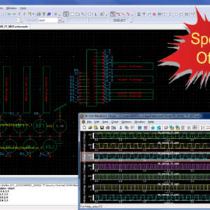
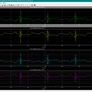
List of the following materials will be included with the Downloaded Backup:A 7T Security Oriented SRAM Bitcell
Abstract:
Power analysis (PA) attacks have become a serious threat to security systems by enabling secret data extraction through the analysis of the current consumed by the power supply of the system. Embedded memories, often implemented with six-transistor (6T) static random access memory (SRAM) cells, serve as a key component in many of these systems. However, conventional SRAM cells are prone to side-channel power analysis attacks due to the correlation between their current characteristics and written data. To provide resiliency to these types of attacks, we propose a security-oriented 7T SRAM cell, which incorporates an additional transistor to the original 6T SRAM implementation and a two-phase write operation, which significantly reduces the correlation between the stored data and the power consumption during write operations. The proposed 7T SRAM cell was implemented in a 28 nm technology and demonstrates over 1000× lower write energy standard deviation between write ‘1’ and ‘0’ operations compared to a conventional 6T SRAM. In addition, the proposed cell has a 39%–53% write energy reduction and a 19%–38% reduced write delay compared to other power analysis resistant SRAM cells.
List of the following materials will be included with the Downloaded Backup:A 9T SRAM Computation-in-Memory Architecture with High-Precision MAC
To address the data-intensive demands of modern artificial intelligence (AI) systems, computation-in-memory(CIM) based on static random-access memory (SRAM) has emerged as a promising solution by integrating computing functionality within memory arrays. However, conventional SRAM CIM architectures face two key limitations: low output resistance in single-transistor transmission paths and voltage instability on charge-sharing bitlines. These limitations collectively degrade computational accuracy to 4–5 LSB-level integral nonlinearity (INL), restricting practical deployment. This work proposes a regulated-cascode 9T SRAM cell that enhances analog computation accuracy using a high-impedance transmission path through a cascode configuration and stabilizing the discharge amount of the bitline from a single cell via active feedback regulation. Implemented in Semiconductor Manufacturing International Corporation (SMIC) 55-nm CMOS technology, the proposed cell demonstrates 1.31 LSB INL at 400-mV bitline swing (68.4% improvement versus 4–5 LSB baselines), achieving 66.7% voltage utilization efficiency compared with the conventional 50% limit and 23.04% frequency improvement is achieved compared with the conventional architecture. It also achieves an energy efficiency of 18.47 fJ/bit and a compact area of 2.655 × 1.175 µm, while demonstrating a classification accuracy of 97.7% on the MNIST dataset. Index Terms Analog linearity enhancement, multirow readout, regulated cascode circuits, static random-access memory (SRAM)-based compute-in-memory, voltage utilization efficiency.
List of the following materials will be included with the Downloaded Backup:A Compact 0.3 V Class AB Bulk Driven OTA
Abstract:
In this article, a new solution for an ultralow-voltage (ULV) ultralow-power (ULP) operational transconductance amplifier (OTA) is presented. Thanks to the combination of a low-voltage bulk-driven nontailed differential stage with the multipath Miller zero compensation technique, a simple class AB power-efficient ULV structure has been obtained, which can operate from supply voltages less than the threshold voltages of the employed MOS transistors, while offering rail-to-rail input common-mode range at the same time. The proposed OTA was fabricated using the 180-nm CMOS process from Taiwan Semiconductor Manufacturing Company (TSMC) and can operate from VDD ranging from 0.3 to 0.5 V. The 0.3-V version dissipates only 12.6 nW of power while showing a 64.7-dB voltage gain at 1-Hz, 2.96-kHz gain-bandwidth product, and a 4.15-V/ms average slew-rate at 30-pF load capacitance. The measured results agree well with simulations.
List of the following materials will be included with the Downloaded Backup:A Fast and Energy-Efficient Level Shifter with Complementary Output Buffer for Energy-Constrained Systems
This brief presents a 55-nm level shifter (LS) that enables wide voltage range conversion from 80 mV to 1.2 V with high energy efficiency and fast transition speed. The proposed design incorporates a complementary output buffer and an assist discharge path to suppress the short-circuit current and enhance the transition speed. A multi threshold transistor strategy is adopted to expand the input range and reduce static power. Measurement results across 15 samples demonstrate robust subthreshold performance with 4.4-ns transition delay and 49.1-fJ/transition energy during 0.3–1.2-V conversion at 1 MHz. The measured average minimum convertible input voltages are 80 and 139 mV at input frequencies of 50 kHz and 1 MHz, respectively. The compact layout occupies only 7.96 µm 2. Compared to the best benchmarked prior work, the proposed LS achieves 33.8% improvement in energy-delay metrics, making it a highly efficient and scalable solution for energy constrained systems and the Internet of Things (IoT). Index Terms: Current mirror (CM), dual supply, level shifter (LS), low power, subthreshold.
List of the following materials will be included with the Downloaded Backup:A Fully Digital Front End Architecture for ECG Acquisition System with 0.5 V Supply
This paper presents a new power-efficient electrocardiogram acquisition system that uses a fully digital architecture to reduce the power consumption and chip area. The proposed architecture is compatible with digital CMOS technology and is capable of operating with a low supply voltage of 0.5 V. In this architecture, no analog block, e.g., low-noise amplifier (LNA), and filters, and no passive elements, such as ac coupling capacitors, are used. A moving average voltage-to time converter is used, which behaves instead of the LNA and anti-aliasing filter. A digital feedback loop is employed to cancel the impact of the dc offset on the circuit, which eliminates the need for coupling capacitors. The proposed architecture of this paper area and power consumption is analysis using tanner tool.
List of the following materials will be included with the Downloaded Backup:A Fully Static Topologically Compressed 21 Transistor Flip Flop With 75 Percentage of Power Saving
An extremely low-power flip-flop (FF) named topologically-compressed flip-flop (TCFF) is proposed. As compared with conventional FFs, the FF reduces power dissipation by 75% at 0% data activity. This power reduction ratio is the highest among FFs that have been reported so far. The reduction is achieved by applying topological compression method, merger of logically equivalent transistors to an unconventional latch structure. The very small number of transistors, only three, connected to clock signal reduces the power drastically, and the smaller total transistor count assures the same cell area as conventional FFs. In addition, fully static full-swing operation makes the cell tolerant of supply voltage and input slew variation. An experimental chip design with 40 nm CMOS technology shows that almost all conventional FFs are replaceable with proposed FF while preserving the same system performance and layout area. The proposed design is analysis the power and delay by using tanner tools.
List of the following materials will be included with the Downloaded Backup:
A High Performance FIR Filter Architecture for Fixed and Reconfigurable Applications
Abstract:
Transpose form finite-impulse response (FIR)filters are inherently pipelined and support multiple constant multiplications (MCM) technique that results in significant saving of computation. However, transpose form configuration does not directly support the block processing unlike direct form configuration. In this paper, we explore the possibility of realization of block FIR filter in transpose form configuration for area-delay efficient realization of large order FIR filters for both fixed and reconfigurable applications. Based on a detailed computational analysis of transpose form configuration of FIR filter, we have derived a flow graph for transpose form block FIR filter with optimized register complexity. A generalized block formulation is presented for transpose form FIR filter. We have derived a general multiplier-based architecture for the proposed transpose form block filter for reconfigurable applications. A low-complexity design using the MCM scheme is also presented for the block implementation of fixed FIR filters. The proposed structure involves significantly less area delay product (ADP) and less energy per sample (EPS) than the existing block implementation of direct-form structure for medium or large filter lengths, while for the short-length filters, the block implementation of direct-form FIR structure has less ADP and less EPS than the proposed structure. The proposed architecture of this paper analysis the logic size, area and power consumption using Xilinx 14.2.
List of the following materials will be included with the Downloaded Backup:A High Resolution FPGA TDC Converter with 2.5 ps Bin Size and -3.79~6.53 LSB Integral Non linearity
Abstract:
As a traditional digital platform, Field Programmable Gate Array (FPGA) is seldom used for analog applications. Since there is no way to fine tune the gate property or circuit structure, the performance of FPGA analog application is usually inferior to its counterparts based on full-custom or even cell-based design. Nevertheless, a high performance FPGA time-to-digital Converter (TDC) is proposed in this paper to expand the FPGA territory into high-end analog applications. The test time signal is sampled by a serious timing references generated by feeding the original clock into a tapped delay line. According to periodicity, the delays among those timing references are wrapped into a single reference period and the effective TDC resolution can be made much smaller than the clock period to compete even with the state-of the art full-custom TDCs in performance. After measurement, the effective resolution is as fine as 2.5 ps. The corresponding differential nonlinearity (DNL) is -1.90~1.66 LSB and the integral nonlinearity (INL) is -3.79~6.53 LSB only.
List of the following materials will be included with the Downloaded Backup:A High-Throughput VLSI Architecture for Hard and Soft SC-FDMA MIMO Detectors
Abstract:
A novel low-complexity multiple-input multiple-output (MIMO) detector tailored for single-carrier frequency division-multiple access (SC-FDMA) systems, suitable for efficient hardware implementations. The proposed detector starts with an initial estimate of the transmitted signal based on a minimum mean square error (MMSE) detector. Subsequently, it recognizes less reliable symbols for which more candidates in the constellation are browsed to improve the initial estimate. The proposed architecture of this paper analysis the logic size, area and power consumption using Xilinx 14.2.
List of the following materials will be included with the Downloaded Backup:A Lightweight True Random Number Generator for Root of Trust Applications
Base Paper Abstract:
There are many schemes proposed to protect integrated circuits (ICs) against an unauthorized access and usage, or at least to mitigate security risks. They lay foundations for hardware roots of trust whose crucial security primitives are generators of truly random numbers. In particular, such generators are used to yield one-time challenges (nonces) supporting the IC authentication protocols employed to counteract potential threats such as untrusted users accessing ICs. However, IC vendors raise several concerns regarding the complexity of these solutions, both in terms of area overhead, the impact on the design flow, and testability. These concerns have motivated this work presenting a simple, yet effective, all-digital lightweight and self-testable random number generator to produce a nonce. It builds on a generic ring generator architecture, i.e., an area and time optimized version of a linear feedback shift register, driven by a multiple-output ring oscillator. A comprehensive evaluation, based on three statistical test suits from NIST and BSI, show feasibility and efficiency of the proposed scheme and are reported herein.
List of the following materials will be included with the Downloaded Backup:A Low Cost Low Power All Digital Spread Spectrum Clock Generator
Abstract:
In this brief, a low-cost low-power all-digital spread spectrum clock generator (ADSSCG) is presented. The proposed ADSSCG can provide an accurate programmable spreading ratio with process, voltage, and temperature variations. To maintain the frequency stability while performing triangular modulation, the fast-relocked mechanism is proposed. The proposed fast-relocked ADSSCG is implemented in a standard performance 90-nm CMOS process, and the active area is 200 µm × 200 µm. The experimental results show that the electromagnetic interference reduction is 14.61 dB with a 0.5% spreading ratio and 19.69 dB with a 2% spreading ratio at 270 MHz The power consumption is 443 µW at 270 MHz with a 1.0 V power supply.
List of the following materials will be included with the Downloaded Backup:A Low Power and High Speed Voltage Level Shifter Based on a Regulated Cross Coupled Pull Up Network
Abstract:
In this brief, a fast and very low power voltage level shifter (LS) is presented. By using a new regulated cross-coupled (RCC) pull-up network, the switching speed is boosted and the dynamic power consumption is highly reduced. The proposed (LS) has the ability to convert input signals with voltage levels much lower than the threshold voltage of a MOS device to higher nominal supply voltage levels. The presented LS occupies a small silicon area owing to its very low number of elements and is ultra-low-power, making it suitable for low-power applications such as implantable medical devices and wireless sensor networks. Results of the post-layout simulation in a standard 0.18-μm CMOS technology show that the proposed circuit can convert up input voltage levels as low as 80 mV. The power dissipation and propagation delay of the proposed level shifter for a low/high supply voltages of 0.4/1.8 V and input frequency of 1 MHz are 123.1 nW and 23.7 ns, respectively.
List of the following materials will be included with the Downloaded Backup:A Low-Voltage Radiation-Hardened 13T SRAM Bit cell for Ultralow Power Space Applications
Proposed Abstract:
Continuous transistor scaling, coupled with the growing demand for low-voltage, low-power applications, increases the susceptibility of VLSI circuits to soft-errors, especially when exposed to extreme environmental conditions, such as those encountered by space applications. The most vulnerable of these circuits are memory arrays that cover large areas of the silicon die and often store critical data. Radiation hardening of embedded memory blocks is commonly achieved by implementing extremely large bitcells or redundant arrays and maintaining a relatively high operating voltage; however, in addition to the resulting area overhead, this often limits the minimum operating voltage of the entire system leading to significant power consumption. In this paper, we propose the first radiation-hardened static random access memory (SRAM) bitcell targeted at low-voltage functionality, while maintaining high soft-error robustness. A 32×32 bit memory macro was designed and fabricated in a standard 0.13-µm CMOS process, showing full read and write functionality down to the subthreshold voltage of 300 mV. This is achieved with a cell layout that is only 2×larger than a reference 6T SRAM cell drawn with standard design rules. The proposed architecture of this paper is analysis the logic size, area and power consumption using tanner tool.
List of the following materials will be included with the Downloaded Backup:A Lower Power Reduced Error Lower Part OR Adder for Multimedia Applications
With the use of multimedia applications, machine learning, and signal processing, approximate computing has become increasingly popular in the pursuit of power-efficient and high-performance architectures for mobile devices. The arithmetic unit is the key component that determines the performance of the overall design. Therefore, in this paper, a novel low-power reduced error lower part-OR adder (RELOA) is proposed. In the proposed architectures, the input bits are divided into three parts, and the sum is computed accurately or approximately based on their significance in the overall sum. The sum of the most significant bits is calculated accurately to have better design metrics, while the least significant bits are approximately to reduce implementation complexity. The proposed architecture offers 16% less power and 9.37% reduction in error metric over existing adders while maintaining a similar delay. Additionally, when processing digital images, the proposed architecture displays good image quality comparable to existing approximate adders.
List of the following materials will be included with the Downloaded Backup:A Nanopower Biopotential Lowpass Filter Using Subthreshold Current-Reuse Biquads With Bulk Effect Self-Neutralization
Abstract:
A nanopower CMOS 4th-order lowpass filter suitable for biomedical applications is presented. The filter is formed by cascading two types of subthreshold current-reuse biquadratic cell. Each proposed cell is capable of neutralizing the bulk effect that induces the passband attenuation. The nearly 0-dB passband gain can thus be maintained, while the entire filter circuit remains compact and power-efficient. Designed for electrocardiogram detection as an example of application, the filter prototype has been fabricated in a 0.35 µm CMOS process occupying 269 µm × 383 µm chip area. Measurements verify that the filter can operate from a 1.5-V single supply and consumes 5.25 nW, while providing a cutoff frequency of 100 Hz and input-referred noise of 39.38 µVrms. The intermodulation-free dynamic range of 51.48 dB is obtained from a two-tone test of 50 and 60 Hz input frequencies. Compared with state-of-the-art nanopower lowpass filters using the most relevant and reasonable figure of merit, the proposed filter ranks the best.
List of the following materials will be included with the Downloaded Backup:A Reliable Low Standby Power 10T SRAM Cell With Expanded Static Noise Margins
Abstract:
This paper explores a low standby power 10T (LP10T) SRAM cell with high read stability and write-ability (RSNM/WSNM/WM). The proposed LP10T SRAM cell uses a strong cross-coupled structure consisting standard inverter with a stacked transistor and Schmitt-trigger inverter with a double-length pull-up transistor. This along with the read path separated from true internal storage nodes eliminates the read-disturbance. Furthermore, it performs its write operation in pseudo differential form through write bit line and control signal with a write-assist technique. To estimate the proposed LP10T SRAM cell’s performance, it is compared with some state-of-the-art SRAM cells using HSPICE in 16-nm CMOS predictive technology model at 0.7 V supply voltage under harsh manufacturing process, voltage, and temperature variations. The proposed SRAM cell offers 4.65X/1.57X/1.46X improvement in RSNM/WSNM/WM and 4.40X/1.69X narrower spread in RSNM/WM compared to the conventional 6T SRAM cell. Furthermore, it shows 1.26X/1.08X/1.01X higher RSNM/WSNM/WM and 1.71X/1.25X tighter/wider spread in RSNM/WM compared to the best studied SRAM cells. The proposed SRAM cell indicates 74.48%/1.41% higher/lower read/write delay compared to the 6T SRAM cell. Moreover, it exhibits the third-(second-) best read (write) dynamic power, consuming 29.69% (26.87%) lower than the 6T SRAM cell. The leakage power is minimized by the proposed design, which is 37.35% and 12.08% lower than that of the 6T and best studied cells, respectively. Nonetheless, the proposed LP10T SRAM cell occupies 1.313X higher area compared to the 6T SRAM cell.
List of the following materials will be included with the Downloaded Backup:A Sub-200nW All-in-One Bandgap Voltage and Current Reference without Amplifiers
Abstract:
This brief presents a low-power and high-precision bandgap voltage and current reference (BGVCR) in one simple circuit for battery-powered applications. All the amplifiers have been eliminated in the proposed circuit. The voltage reference is derived from the bandgap topology, and the current reference is obtained by summing a proportional-to-absolute-temperature (PTAT) current and a complementary-to-absolute-temperature (CTAT) current. Therefore, the temperature coefficient of the current reference can be optimized. Besides, a pseudo-cascode structure and a simple line sensitivity enhancement circuit are adopted to improve the current mirror accuracy and line sensitivity. The proposed circuit is fabricated in a 0.18-μm deep N-well CMOS process with an active area of 0.063 mm2. The measured VREF and IREF are 1.2 V and 51 nA, respectively. The VREF and IREF show measured average temperature coefficients of 32.7 ppm/℃ and 89 ppm/℃ at a temperature of -45 to 125 ℃ and standard deviations of 0.17 % and 1.15 %, respectively. In the supply voltage range of 2 to 5 V, the line sensitivities of voltage and current are 0.058%/V and 1.76%/V, respectively. The minimum supply voltage is 2 V with a total power consumption of 192 nW at room temperature.
List of the following materials will be included with the Downloaded Backup:A System of Two Coupled Oscillators With a Continuously Controllable Phase Shift
Abstract:
We present a novel generalization of quadrature oscillators (QVCO) which we call “arbitrary phase oscillator” or APO for short. In contrast to a QVCO which generates only quadrature phases, the APO is capable of continuously generating any desired phase at its output. The proposed structure employs a novel coupling mechanism to generate arbitrary phase shifts between two coupled oscillators without the need for an explicit phase shifter. A rigorous nonlinear dynamic analysis is presented to give a closed-form formula for the generated phase shifts, and the theory is verified by numerical simulation as well as measurement results of a prototype chip fabricated in 130-nm CMOS technology. The prototype APO has a frequency tuning range of 4.90–5.65 GHz and is continuously phase tunable from 0◦ to 360◦ across the entire frequency range. The APO structure can be used in designing novel coupled-oscillator-based phased arrays for 5G wireless communications.
List of the following materials will be included with the Downloaded Backup:A Thermal Energy Harvesting Power Supply with an Internal Start up Circuit
A complete thermal energy harvesting power supply for implantable pacemakers is presented in this paper. The designed power supply includes an internal startup and does not need any external reference voltage. The startup circuit includes a prestart up charge pump (CP) and a startup boost converter. The prestart up CP consists of an ultralow-voltage oscillator followed by a high-efficiency modified Dickson. Forward body biasing is used to effectively reduce the MOS threshold voltages as well as the supply voltage in oscillator and CP. The steady-state circuit includes a high-efficiency boost converter that utilizes a modified maximum power point tracking scheme. The system is designed so that no failure occurs under overload conditions. Using this approach, a thermal energy harvesting power supply has been designed using 130-nm CMOS technology with low dropout regulator. Finally we are got the output of 2.5V in 10ms.
List of the following materials will be included with the Downloaded Backup:
A Three Stage Comparator and Its Modified Version With Fast Speed and Low Kickback
Abstract:
This brief presents a three-stage comparator and its modified version to improve the speed and reduce the kickback noise. Compared to the traditional two-stage comparators, the three-stage comparator in this work has an extra amplification stage, which enlarges the voltage gain and increases the speed. Unlike the traditional two-stage structure that uses pMOS input pair in the regeneration stage, the three-stage comparator makes it possible to use nMOS input pairs in both the regeneration stage and the amplification stage, further increasing the speed. Furthermore, in the proposed modified version of three-stage comparator, a CMOS input pair is adopted at the amplification stage. This greatly reduces the kickback noise by canceling out the nMOS kickback through the pMOS kickback. It also adds an extra signal path in the regeneration stage, which helps increase the speed further. For easy comparison, both the conventional two-stage and the proposed three-stage comparators are implemented in the same 130-nm CMOS process. Measured results show that the modified version of three-stage comparator improves the speed by 32%, and decreases the kickback noise by ten times. This improvement is not at the cost of increased input referred offset or noise.
List of the following materials will be included with the Downloaded Backup:A Two-Stage CMOS Amplifier with High Degree of Stability for All Capacitive Loads
This article presents the conception, design, and realization of a fully differential two-stage CMOS amplifier, that is, unconditionally stable for any value of the capacitive load. This is simply achieved by sending a scaled replica of the output stage current to the amplifier virtual ground in order to create a left half-plane (LHP) zero in the loop gain that either cancels or tracks the output pole in all process, voltage, and temperature (PVT) conditions. Consequently, from a stability point of view, the amplifier behaviour resembles that of a single-pole OTA. Starting from an existing two-stage gain-programmable amplifier, designed in a 0.18-µm bipolar-CMOS-DMOS (BCD) process that was able to drive only 10 pF without encountering into stability issues, a simple circuit has been added to extend the stability to any capacitive load value. An interesting and unusual method, based on the frequency behaviour of the unloaded closed-loop amplifier output impedance, has been introduced to further verify the unconditional stability of this solution. Measurements show a high degree of stability in any load conditions. In the used 0.18-µm BCD technology, silicon area and current consumption of the extra circuit are only 0.0004 mm and 2 µA, respectively, with a 5-V power supply.
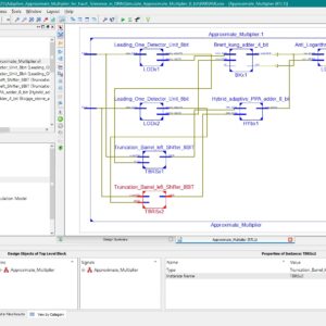
List of the following materials will be included with the Downloaded Backup:AdAM: Adaptive Approximate Multiplier for Fault Tolerance in DNN Accelerators
Base Paper Abstract:
Deep Neural Network (DNN) hardware accelerators are essential in a spectrum of safety-critical edge-AI applications with stringent reliability, energy efficiency, and latency requirements. Multiplication is the most resource-hungry operation in the neural network’s processing elements. This paper proposes a scalable adaptive fault-tolerant approximate multiplier (AdAM) tailored for ASIC-based DNN accelerators at the algorithm and circuit levels. AdAM employs an adaptive adder that relies on an unconventional use of input Leading One Detector (LOD) values for fault detection by optimizing unutilized adder resources. A gate-level optimized LOD design and a hybrid adder design are also proposed as a part of the adaptive multiplier to improve the hardware performance. The proposed architecture uses a lightweight fault mitigation technique that sets the detected faulty bits to zero. The hardware resource utilization and the DNN accelerator’s reliability metrics are used to compare the proposed solution against the Triple Modular Redundancy (TMR) in multiplication, unprotected exact multiplication, and unprotected approximate multiplication. It is demonstrated that the proposed architecture enables a multiplication with a reliability level close to the multipliers protected by TMR while at the same time utilizing 2.74× less area and with 39.06% less power-delay product compared to the exact multiplier. Moreover, it has similar area, delay, and power consumption parameters compared to the state-of-the-art approximate multipliers with similar accuracy while providing fault detection and mitigation capability. Index Terms Deep neural networks, approximate computing, circuit design, reliability, DNN accelerator.
List of the following materials will be included with the Downloaded Backup:Algorithm and Architecture for a Low Power Content Addressable Memory Based on Sparse Clustered Networks
Abstract: We propose a low-power content-addressable memory (CAM) employing a new algorithm for associativity between the input tag and the corresponding address of the output data of 128bit. The proposed architecture is based on a recently developed sparse clustered network using binary connections that on-average eliminates most of the parallel comparisons performed during a search. Therefore, the dynamic energy consumption of the proposed design is significantly lower compared with that of a conventional low-power CAM design. Given an input tag, the proposed architecture computes a few possibilities for the location of the matched tag and performs the comparisons on them to locate a single valid match. A design methodology based on the silicon area and power budgets, and performance requirements is discussed. The proposed architecture of this paper will be analysis the logic size, area and power consumption using Xilinx 14.2.
List of the following materials will be included with the Downloaded Backup:
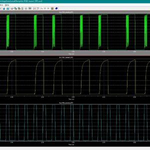
An Area-Efficient Fractional Output Divider Based on Foreground DTC INL Calibration
This brief presents a fractional output divider (FOD) with a foreground digital-to-time converter (DTC) INL calibration scheme. This calibration scheme adjusts the delay control words of two main DTCs (mDTCs) to enable mutual comparison between them. By using a sign-least-mean-squares (sign-LMS) algorithm, the INL error codes are obtained and subsequently applied to a calibration DTC (cDTC) to compensate for the mDTC INL. The prototype occupies a compact core area of 0.01mm2 and operates at a 0.9V supply with a power consumption of 3.6mW at 500MHz. Measurements demonstrate an integrated jitter of 512fs (10kHz to 20MHz) and spur level of -70dBc at 123.46MHz. Index Terms—Fractional output divider (FOD), frequency synthesis, digital-to-time converter (DTC), integral nonlinearity (INL), foreground calibration, bang-bang phase detector (BBPD).
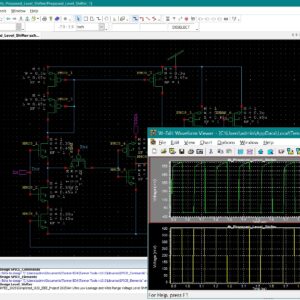
List of the following materials will be included with the Downloaded Backup:An Ultra-Low Leakage and Wide-Range Voltage Level Shifter for Low-Power Digital CMOS VLSIs
Base Paper Abstract:
This brief presents an ultra-low leakage and fast conversion level shifter with wide-range voltage conversion and frequency. The proposed level shifter adopts the leakage shutoff transistors, which can completely cut off the static current when the circuits stand by. The pull-down network employs the low-threshold transistor for the fast fall transition. The proposed level shifter also solves the swing problem and achieves a fast conversion by using the voltage hysteresis transistor, strengthening the pull-up network to ensure the internal node is fast and fully charged. Measurement results based on the 55 nm process show that the average ultra-low leakage of the proposed level shifter is 34.8 pW when converting from 0.3 V input to 1.2 V output. Meanwhile, the average propagation delay and the average energy per transition of the proposed level shifter are 13.86 ns and 22.71 fJ for an input frequency of 1 MHz, respectively. The maximum conversion range is from 0.13 V to 1.2 V. Index Terms: Level shifter, ultra-low power, multi-supply voltage circuit, sub-threshold operation.
List of the following materials will be included with the Downloaded Backup:Analysis, Comparison, and Experimental Validation of a Class AB Voltage Follower With Enhanced Bandwidth and Slew Rate
Abstract:
This paper describes a bandwidth (BW)- and slew rate (SR)-enhanced class AB voltage follower (VF). A thorough small signal analysis of the proposed and a state-of-the-art AB-enhanced VF is presented to compare their performance. The proposed circuit has 50-MHz BW, 19.5-V/µs SR, and a BW figure of merit of 41.6 (MHz × pF/µW) for CL = 50 pF. It provides 13 times higher current efficiency and 15 times higher BW than the conventional VF with equal 60-µW static power dissipation. The experimental and simulation results of a fabricated test chip in the 130-nm CMOS technology validate the proposed circuit.
List of the following materials will be included with the Downloaded Backup:Camouflaged Logic Gates Using Threshold-Voltage-Defined Memory Cells
This brief proposes two types of camouflaged logic gates using threshold-voltage-defined memory cells (TVD-MCs). The proposed multiplexer-select TVD-MC (MS-TVDMC) gate consists of a target logic gate, several camouflage logic gates, a multiplexer (MUX), and TVD-MCs. All logic gates and MUX are implemented with standard threshold-voltage transistors. The TVD-MC is composed of two cross coupled inverters with low- or high-threshold-voltage transistors. When its supply voltage increases from ground to VDD, its data become “0” or “1” according to the threshold voltages of transistors in two inverters. The target logic gate is selected with the MUX by the data stored in the TVD-MCs. The data are defined by the threshold voltages of transistors, so that it is difficult to distinguish the target logic gate from the other camouflage logic gates. The proposed logic-merged TVD-MC (LM-TVDMC) gate merges all logic gates and MUX in the MS-TVDMC gate at the transistor level. The proposed camouflaged gates significantly reduce the delay, power consumption, and leakage current compared to the conventional dynamic enhanced-TVD (DE-TVD) camouflaged gate requiring the dynamic power and delay overheads and the conventional threshold-voltage-defined (TVD) switch camouflaged gate with large ON-resistances in switch transistors. Index Terms: Camouflaged gate, logic gate, reverse engineering, security, threshold-voltage-defined (TVD).
List of the following materials will be included with the Downloaded Backup:Chaos-Based Bitwise Dynamical Pseudorandom Number Generator on FPGA
Abstract:
In this paper, a new pseudorandom number generator (PRNG) based on the logistic map has been proposed. To prevent the system to fall into short period orbits as well as increasing the randomness of the generated sequences, the proposed algorithm dynamically changes the parameters of the chaotic system. This PRNG has been implemented in a vertex 7 field-programmable gate array (FPGA) with a 32-bit fixed point precision, using a total of 510 lookup tables (LUTs) and 120 registers. The sequences generated by the proposed algorithm have been subjected to the National Institute of Standards and Technology (NIST) randomness tests, passing all of them. By comparing the randomness with the sequences generated by a raw 32-bit logistic map, it is shown that, by using only an additional 16% of LUTs, the proposed PRNG obtains a much better performance in terms of randomness, increasing the NIST passing rate from 0.252 to 0.989. Finally, the proposed bitwise dynamical PRNG is compared with other chaos-based realizations previously proposed, showing great improvement in terms of resources and randomness.
List of the following materials will be included with the Downloaded Backup:CMOS First-Order All-Pass Filter With 2-Hz Pole Frequency
Abstract:
A CMOS fully integrated all-pass filter with an extremely low pole frequency of 2 Hz is introduced in this paper. It has 0.08-dB passband ripple and 0.029-mm2Si area. It has 0.38-mW power consumption in strong inversion with ±0.6-V power supplies. In subthreshold, it has 0.64-µW quiescent power and operates with ±200-mV dc supplies. Miller multiplication is used to obtain a large equivalent capacitor without excessive Si area. By varying the gain of the Miller amplifier, the pole frequency can be varied from 2 to 48 Hz. Experimental and simulation results of a test chip prototype in 130-nm CMOS technology validate the proposed circuit.
List of the following materials will be included with the Downloaded Backup:Column-Selection-Enabled 10T SRAM Utilizing Shared Diff-VDD Write and Dropped-VDD Read for Power Reduction
Abstract:
A non-destructive column-selection-enabled 10T SRAM for aggressive power reduction is presented in this brief. It frees a half-selected behavior by exploiting the bit line-shared data-aware write scheme. The differential-VDD (Diff-VDD) technique is adopted to improve the write ability of the design. In addition, its decoupled read bit lines are given permission to be charged and discharged depending on the stored data bits. In combination with the proposed dropped-VDD biasing, it achieves the significant power reduction. The experimental results show that the proposed design provides the 3.3× improvement in the write margin compared with the standard Diff-10T SRAM. A 5.5-kb 10T SRAM in a 65-nm CMOS process has a total power of 51.25 µW and a leakage power of 41.8 µW when operating at 6.25 MHz at 0.5 V, achieving 56.3% reduction in dynamic power and 32.1% reduction in leakage power compared with the previous single-ended 10T SRAM.
List of the following materials will be included with the Downloaded Backup:Design and analysis of Reversible Approximate Full Adder and its applications with Optimized 4:2, 5:2, 7:2 Compressors for Efficient Approximate Multipliers
Design and Application of Mean and Square Root Circuits for Stochastic Computing
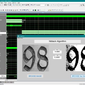
Stochastic computing (SC) is an unconventional computing paradigm that represents values using probabilities. This representation enables simple logic gates to perform complex arithmetic operations. This brief proposes two low hardware-cost stochastic mean circuits for even and odd inputs, respectively, along with a high-accuracy stochastic square root circuit. The circuits are designed by considering correlation technique and achieve excellent performance. Experimental results demonstrate that the proposed mean circuits surpass previous counterparts in computing accuracy and hardware cost. For instance, the proposed 9-input mean circuit can achieve at least an 86.7% reduction in mean square error (MSE) and a 28.6% reduction in area. For the square root circuit, the proposed design achieves a reduction in MSE of at least 19.6%. The proposed circuits are further demonstrated with the Niblack binarization algorithm, which shows superior performance of accuracy. Index Terms: Stochastic computing, mean circuit, square root circuit, binarization processing.
List of the following materials will be included with the Downloaded Backup:Design and Implementation of Arithmetic Logic Unit in DSCH3 and Microwind
Proposed Abstract:
The Arithmetic Logic Unit (ALU) is a fundamental component in digital systems, particularly in the central processing units (CPUs) of microprocessors, where it executes essential arithmetic and logical functions. This paper presents the design and implementation of an 8-bit Arithmetic Logic Unit (ALU) using CMOS technology, developed and simulated in DSCH3 and Microwind environments. The primary goal of this research is to design an efficient and compact ALU optimized for performance and area efficiency. The 8-bit ALU performs eight operations: ripple carry addition, ripple borrow subtraction, multiplication, XOR, left shift, right shift, NAND, and NOR. Each logic gate within the ALU is constructed using CMOS logic to enhance power efficiency and integration density. This paper provides a detailed description of the ALU's CMOS-based architecture, its key components, and the control mechanism for operation selection. Performance metrics, including speed, area efficiency, and power consumption, are analyzed to assess the ALU’s effectiveness in CMOS technology.
List of the following materials will be included with the Downloaded Backup:Design Methodology for Voltage Scaled Clock Distribution Networks
Abstract:
A low-voltage/swing clocking methodology is developed through both circuit and algorithmic innovations. The primary objective is to significantly reduce the power consumed by the clock network while maintaining the circuit performance the same. a novel D-flip-flop (DFF) cell that maximizes power savings by enabling low-voltage/swing operation throughout the entire clock network . In this proposed design of the LSFF is consume the less power compare to existing design. The proposed architecture of this paper is analysis the logic size, area and power consumption using tanner tool.
List of the following materials will be included with the Downloaded Backup:Design of 4-bit Ripple carry adder and using 9T full adder
Design of a Hardware Efficient Approximate 4-2 Compressor for Multiplication in Image Processing
Base Paper Abstract:
This letter presents a novel hardware-efficient approximate 4-2 compressor design that significantly enhances accuracy through a systematic analysis of input patterns obtained from practical applications. We incorporate a majority operation and a compound gate in the compressor design to effectively boost hardware efficiency in multiplications. Our design approach results in substantial error reductions, with normalized mean error distance (NMED) and mean relative error distance (MRED) decreasing by up to 74.84% and 82.04%, respectively, compared to existing approximate multipliers discussed in this letter. When implemented in a 32-nm CMOS technology, the approximate multiplier adopting the proposed 4-2 compressor achieves excellent hardware efficiency, reducing area, power, and energy consumption by up to 8.95%, 13.02%, and 13.02%, respectively, compared to the other alternatives. Moreover, our design delivers enhanced performance in image processing tasks, achieving up to a 4.84× increase in peak signal-to-noise ratio (PSNR) compared to other designs, all while optimizing hardware efficiency. Index Terms—Approximate multiplier, majority operation, compound gate, image processing, approximate 4-2 compressor.
List of the following materials will be included with the Downloaded Backup:Design of a Low-Power Analog Integrated Deep Convolutional Neural Network
Base Paper Abstract:
In this article, a framework for the analog implementation of a deep convolutional neural network (CNN) is introduced and used to derive a new circuit architecture which is composed of an improved analog multiplier and circuit blocks implementing the ReLU activation function and the argmax operator. The operating principles of the individual blocks, as well as those of the complete architecture, are analysed and used to realize a low-power analog classifier, consuming less than 1.8 µW. The proper operation of the classifier is verified via a comparison with a software equivalent implementation and its performance is evaluated against existing circuit architectures. The proposed architecture is implemented in a TSMC 90-nm CMOS process and simulated using Cadence IC Suite for both schematic and layout design. Corner and Monte Carlo mismatch simulations of the schematic and the physical circuit (post layout) were conducted to evaluate the effect of transistor mismatches and process voltage temperature (PVT) variations and to showcase a proposed systematic method for offsetting their effect.
List of the following materials will be included with the Downloaded Backup:Design of a Scalable Low Power 1 bit Hybrid Full Adder for Fast Computation
Abstract:
A novel design of a hybrid Full Adder (FA) using Pass Transistors (PTs), Transmission Gates (TGs) and Conventional Complementary Metal Oxide Semiconductor (CCMOS) logic is presented. Performance analysis of the circuit has been conducted using Cadence toolset. For comparative analysis, the performance parameters have been compared with twenty existing FA circuits. The proposed FA has also been extended up to a word length of 64 bits in order to test its scalability. Only the proposed FA and five of the existing designs have the ability to operate without utilizing buffer in intermediate stages while extended to 64 bits. According to simulation results, the proposed design demonstrates notable performance in power consumption and delay which accounted for low power delay product. Based on the simulation results, it can be stated that the proposed hybrid FA circuit is an attractive alternative in the data path design of modern high-speed Central Processing Units.
List of the following materials will be included with the Downloaded Backup:Design of Area-Efficient and Highly Reliable RHBD 10T Memory Cell for Aerospace Applications
Abstract:
In this brief, based on upset physical mechanism together with reasonable transistor size, a robust 10T memory cell is first proposed to enhance the reliability level in aerospace radiation environment, while keeping the main advantages of small area, low power, and high stability. Using Taiwan Semiconductor Manufacturing Company 65-nmCMOS commercial standard process, simulations performed in Cadence Spectre demonstrate the ability of the proposed radiation-hardened-by-design 10T cell to tolerate both 0 →1and1→0 single node upsets, with the increased read/write access time.
List of the following materials will be included with the Downloaded Backup:Design of Low Power High Performance 2-4 and 4-16 Mixed-Logic Line Decoders
Abstract:
This paper introduces a mixed-logic design method for line decoders, combining transmission gate logic, pass transistor dual-value logic and static CMOS. Two novel topologies are presented for the 2-4 decoders: a 14-transistor topology aiming on minimizing transistor count and power dissipation and a 15-transistor topology aiming on high power delay performance. Both a normal and an inverting decoder are implemented in each case, yielding a total of four new designs. Furthermore, four new 4-16 decoders are designed, by using mixed-logic 2-4 pre decoders combined with standard CMOS post-decoder. All proposed decoders have full swinging capability and reduced transistor count compared to their conventional CMOS counterparts. Finally, a variety of comparative spice simulations at the 32 nm shows that the proposed circuits present a significant improvement in power and delay, outperforming CMOS in almost all cases.
List of the following materials will be included with the Downloaded Backup:Design of Low-Power and Area Efficient ECG Low Pass Filter Using VSCP
Electrocardiogram (ECG) signal processing is a core requirement in wearable and portable healthcare systems, where long battery life, compact hardware, and reliable signal quality are increasingly demanded by modern medical applications. The aim of this work is to address the challenge of designing an energy-efficient and area-optimized ECG low-pass filter capable of suppressing high-frequency noise while preserving diagnostically important cardiac information in advanced CMOS technology. To achieve this, a low-pass filter based on a vertical source-coupled pair (VSCP) transconductance architecture is proposed, in which the circuit topology and biasing strategy are carefully optimized to suit ECG signal bandwidth and low-voltage operation. The architectural novelty of this work lies in the adaptation and refinement of a VSCP-based transconductance structure into an ECG-specific low-pass filter with reduced transistor count, improved linearity, and enhanced power efficiency in a 45-nm CMOS process. The proposed filter supports essential ECG signal conditioning functions, including low-frequency passband preservation, effective attenuation of out-of-band noise, and stable operation under low-power constraints. The design is implemented and simulated using Tanner EDA tools, and realistic ECG input signals generated from the MIT-BIH database are applied to validate functional performance. Simulation results demonstrate that the proposed filter achieves notable reductions in power consumption and silicon area compared to conventional ECG low-pass filter designs, while maintaining reliable frequency response and low noise, making it well suited for compact and battery-operated ECG monitoring systems.
List of the following materials will be included with the Downloaded Backup:Dual Use of Power Lines for Design for Testability A CMOS Receiver Design
As the circuit complexity increases, the number of internal nodes increases proportionally, and individual internal nodes are less accessible due to the limited number of available I/O pins. To address the problem, we proposed power line communications (PLCs) at the IC level, specifically the dual use of power pins and power distribution networks for application/ observation of test data as well as delivery of power. A PLC receiver presented in this paper intends to demonstrate the proof of concept, specifically the transmission of data through power lines. The main design objective of the proposed PLC receiver is the robust operation under variations and droops of the supply voltage rather than high data speed. The PLC receiver is designed and fabricated in CMOS 0.18-µm technology under a supply voltage of 1.8V.
List of the following materials will be included with the Downloaded Backup:
Efficient TCAM Design Based on Multipumping Enabled Multiported SRAM on FPGA
Abstract:
Ternary content-addressable memory (TCAM)-based search engines play an important role in networking routers. The search space demands of TCAM applications are constantly rising. However, existing realizations of TCAM on field-programmable gate arrays (FPGAs) suffer from storage inefficiency. This paper presents a multipumping-enabled multiported SRAM-based TCAM design on FPGA, to achieve an efficient utilization of SRAM memory. Existing SRAM-based solutions for TCAM reduce the impact of the increase in the traditional TCAM pattern width from an exponential growth in memory usage to a linear one using cascaded block RAMs (BRAMs) on FPGA. However, BRAMs on state-of-the-art FPGAs have a minimum depth limitation, which limits the storage efficiency for TCAM bits. Our proposed solution avoids this limitation by mapping the traditional TCAM table divisions to shallow sub-blocks of the configured BRAMs, thus achieving a memory-efficient TCAM memory design. The proposed solution operates the configured simple dual-port BRAMs of the design as multiported SRAM using the multipumping technique, by clocking them with a higher internal clock frequency to access the sub-blocks of the BRAM in one system cycle. We implemented our proposed design on a Virtex-6 xc6vlx760 FPGA device. Compared with existing FPGA-based TCAM designs, our proposed method achieves up to 2.85 times better performance per memory.
List of the following materials will be included with the Downloaded Backup:Energy-Efficient Buffer-Based Ternary SRAM Cell With Application to Image Processing
Base Paper Abstract:
This paper presents a design of a variation-resilient and energy-efficient ternary memory cell (TSRAM) suited for power-demanding internet-of-things (IoT) applications that run on batteries. The TSRAM cell utilizes a latch composed of an efficient ternary buffer (TBUF) with positive feedback, a single bit line, and a transmission gate for switching access, with an overall area only about 39% more than binary 6T SRAM. The threshold voltage (Vth) tuning of carbon nanotube field-effect transistor (CNTFET) devices has been explored to achieve the three storage levels. Simulations were conducted using the standard Stanford 32-nm CNTFET model file in the Synopsis HSPICE simulator. The projected design offers substantial reductions of 54.94% in real power, 67.06% in write power, and 21.59% in area compared to the best buffer-based TSRAM designs. These power savings are achieved by minimizing the transistor count and eliminating any direct current path between VDD and ground in the TBUF design for getting logic ‘1’. Furthermore, the proposed design demonstrates the highest logic ‘1’ static noise margin (SNM1) and shows resilience to process, voltage, and temperature (PVT) variations. The TSRAM electrical quality matrix (TEQM), a crucial figure of merit, indicates the superior performance of the proposed design for IoT applications. The study was further extended to conduct simulations and report the performance metrics of the proposed TSRAM array. Ultimately, to evaluate the real-world application of the triple memory structures, the pixel-by-pixel storage process of a grayscale image with three-value data content is performed based on a hardware algorithm. The obtained results demonstrate that the proposed TSRAM architecture has about a 26.3% improvement in hardware performance compared to its highest performing counterpart scheme.
List of the following materials will be included with the Downloaded Backup:Energy-Quality Scalable Adders Based on Non-zeroing Bit Truncation
Abstract:
Approximate addition is a technique to trade off energy consumption and output quality in error-tolerant applications. In prior art, bit truncation has been explored as a lever to dynamically trade off energy and quality. In this brief, an innovative bit truncation strategy is proposed to achieve more graceful quality degradation compared to state-of-the-art truncation schemes. This translates into energy reduction at a given quality target. When applied to a ripple-carry adder, the proposed bit truncation approach improves quality by up to 8.5 dB in terms of peak signal-to-noise ratio, compared to traditional bit truncation. As a case study, the proposed approach was applied to a discrete cosine transform engine. In comparison with prior art, the proposed approach reduces energy by 20%, at insignificant delay and silicon area overhead.
List of the following materials will be included with the Downloaded Backup:Fail Safe Logic Design Strategies Within Modern FPGA Architectures
Fail-safe computing refers to computing systems that revert to a non-operational safe state when a fault occurs. In this paper, we investigate a circuit level technique as mitigation for single event upsets (SEUs) and fault injection attacks on field programmable gate arrays (FPGAs), and analyze the effectiveness of the technique as a fail-safe monitor for an encryption algorithm. The propagation of fault effects through FPGA primitives including lookup tables (LUTs) and programmable interconnect points (PIPs) is assessed within an FPGA architecture created using an open source tool, and validated using fault injection experiments on an FPGA. The analysis reveals additional vulnerabilities exist within reconfigurable architectures over those in equivalent fail-safe application specific integrated circuit (ASIC), thus requiring a more elaborate network of redundant circuits and checking logic. The configuration memory bits (CMBs), which configure routing and designate logic functions within the LUTs of the FPGA, add complexity to fail-safe design strategies by introducing additional fault conditions and fault propagation paths. A resource efficient fail-safe circuit design technique called Design for Fail-safe in reconfigurable systems (DEFCON) is proposed. The benefits and limitations associated with DEFCON are described in the context of fault injection experiments carried out as simulations and in FPGA hardware.
List of the following materials will be included with the Downloaded Backup:FPGA Implementation for Odor Identification with Depthwise Separable Convolutional Neural Network
Base Paper Abstract:
The integrated electronic nose (e-nose) design, which integrates sensor arrays and recognition algorithms, has been widely used in different fields. However, the current integrated e-nose system usually suffers from the problem of low accuracy with simple algorithm structure and slow speed with complex algorithm structure. In this article, we propose a method for implementing a deep neural network for odor identification in a small-scale Field-Programmable Gate Array (FPGA). First, a lightweight odor identification with depthwise separable convolutional neural network (OIDSCNN) is proposed to reduce parameters and accelerate hardware implementation performance. Next, the OI-DSCNN is implemented in a Zynq-7020 SoC chip based on the quantization method, namely, the saturation-flooring KL divergence scheme (SF-KL). The OI-DSCNN was conducted on the Chinese herbal medicine dataset, and simulation experiments and hardware implementation validate its effectiveness. These findings shed light on quick and accurate odor identification in the FPGA.
List of the following materials will be included with the Downloaded Backup:Frequency-Boost Jitter Reduction for Voltage-Controlled Ring Oscillators
Ring oscillators (ROs) are popular due to their small area, modest power, wide tuning range, and ease of scaling with process technology. However, their use in many applications is limited due to poor phase noise and jitter performance. Thermal noise and flicker noise contribute jitter that decreases inversely with oscillation frequency. This paper describes a frequency boost technique to reduce jitter in ROs. We boost the internal oscillation frequency and introduce a frequency divider following the oscillator to maintain the desired output frequency. This approach offers reduced jitter as well as the opportunity to trade off output jitter with power for dynamic performance management. The oscillator has 32 operating modes, corresponding to different values for the ring size and frequency division. In a 0.5-µm CMOS process, the highest oscillation frequency achieved is 25 MHz with a root-mean-square period jitter of 54 ps and a power consumption of 817 µW at 5 V supply. A jitter model for current-starved oscillators was derived and verified by measurement; a direct relationship between oscillation frequency and jitter was derived and measured. Compared with other oscillators, this design achieves the highest performance in terms of jitter per unit interval and figure-of-merit. The performance is expected to improve in more advanced technologies. The results are summarized to offer design guidance based on the frequency boost technique. The proposed architecture of this paper area and power consumption analysis using tanner tool.
List of the following materials will be included with the Downloaded Backup:
Full Swing Local Bitline SRAM Architecture Based on the 22 nm FinFET Technology for Low Voltage Operation
The previously proposed average-8T static random access memory (SRAM) has a competitive area and does not require a write-back scheme. In the case of an average-8T SRAM architecture, a full-swing local bitline (BL) that is connected to the gate of the read buffer can be achieved with a boosted wordline (WL) voltage. However, in the case of an average-8T SRAM based on an advanced technology, such as a 22-nm FinFET technology, where the variation in threshold voltage is large, the boosted WL voltage cannot be used, because it degrades the read stability of the SRAM. Thus, a full-swing local BL cannot be achieved, and the gate of the read buffer cannot be driven by the full supply voltage (VDD), resulting in a considerably large read delay. To overcome the above disadvantage, in this paper, a differential SRAM architecture with a full-swing local BL is proposed. In the proposed SRAM architecture, full swing of the local BL is ensured by the use of cross-coupled pMOSs, and the gate of the read buffer is driven by a full VDD, without the need for the boosted WL voltage. Various configurations of the proposed SRAM architecture, which stores multiple bits, are analyzed in terms of the minimum operating voltage and area per bit. The proposed SRAM that stores four bits in one block can achieve a minimum voltage of 0.42 V and a read delay that is 62.6 times lesser than that of the average-8T SRAM based on the 22-nm FinFET technology. The proposed architecture of this paper is analysis the area and power consumption using tanner tool.
List of the following materials will be included with the Downloaded Backup:
Full-Array Boolean Logic CIM Macro with Self-Recycling 10T-SRAM Cell for AES Systems
Base Paper Abstract:
Computing in memory (CIM), which alleviates the need to transfer a large amount of data between processor and memory, significantly reducing latency and energy consumption, is a promising new computing architecture for addressing the von Neumann bottleneck problem. This article proposes a CIM array structure composed of self-recycling 10T static random access memory (SRAM) cells, which can realize orthogonal data writing, and multiple Boolean logical operations for the entire array. The self-recycling and full-array activation characteristics are extremely suitable for accelerating diverse data processing algorithms such as the Advanced Encryption Standard (AES). A 4-kb SRAM is implemented in 55-nm CMOS technology to verify the effectiveness of the design. Compared with other state-of-threat architectures, the throughput and the operating frequency of the proposed CIM macro are increased to 843 GOPS/kb (2.64×) and 823.7 MHz (2.6×), respectively. The energy efficiency reaches 246.9 TOPS/W. When applied to the AES, the energy consumption is 35.77% less than the digital CIM architecture that is not self-recycling.
List of the following materials will be included with the Downloaded Backup:Gate diffusion input based 4-bit Vedic multiplier design
Abstract:
A multiplier is one of the key hardware blocks in most of the processors. Multiplication is a lengthy, time-consuming task. Vedic multiplication in field programmable gate array implementation has been proven effective in reducing the number of steps and circuit delay. Conventionally at the circuit level, complementary metal oxide semiconductor (CMOS) logic is used to design a multiplier. In CMOS circuits, the area is always an issue. Gate diffusion input (GDI)-based logic has been explored in the literature to reduce the number of transistors for various logic functions. Thus, Vedic mathematics, on the one hand, simplifies the multiplication process and reduces the delay; while on the other hand, GDI technique helps in minimizing the transistor count (TC) and reduction in power. Therefore, this study puts forth a GDI logic-based 4-bit Vedic multiplier. To study the effectiveness of the GDI logic, the transient response of a 2-bit Vedic multiplier using CMOS and GDI is compared. For the 4-bit Vedic multiplier, two design approaches are taken into consideration. The performance of these circuits is analyzed in terms of average power dissipation, delay, and TC. The effect of supply voltage scaling is also studied. The circuit simulations are carried out at 130 nm for bulk metal oxide semiconductor field effect transistor predictive technology model-based device parameters.
List of the following materials will be included with the Downloaded Backup:Glitch Energy Reduction and SFDR Enhancement Techniques for Low Power Binary Weighted Current Steering DAC
This brief proposes a glitch reduction approach by dynamic capacitance compensation of binary-weighted current switches in a current-steering digital-to-analog converter (DAC). The method was proved successfully by a 10-bit 400-MHz pure binary-weighted current steering DAC with a minimum number of retiming latches. The experiment results yield very low-glitch energy during major carry transitions at output.
List of the following materials will be included with the Downloaded Backup:Hardware Efficient Architecture for Multiple Quantized Gaussian Noise Generation
This paper presents two novel architectures to generate a number of quantized Gaussian noises. The first architecture exploits inversion through uniform segmentation, enabling a uniform look up table (LUT) splitting technique to efficiently generate quantized Gaussian noise while maintaining reasonable tail quality in Gaussian noise generation. The second architecture utilizes inversion through hierarchical segmentation and a probability-based LUT selection, significantly reducing the total LUT size while preserving the tail quality of the generated Gaussian noise. Both designs generate multiple uniform random numbers by cascading combinational circuits, which improves Gaussian noise generation efficiency compared to the conventional linear feedback shift register-based method. Compared to the previous architecture based on inversion through hierarchical segmentation, the proposed uniform segmentation architecture achieves a 6.02x improvement, when implemented on a field-programmable gate array device, in terms of throughput per configurable logic block, and the proposed hierarchical segmentation architecture achieves a 2.71x improvement.
List of the following materials will be included with the Downloaded Backup:HDL-Based Modeling Approach for Digital Simulation of Adiabatic Quantum Flux Parametron Logic
Abstract:
AQFP (adiabatic quantum-flux-parametron) circuits are currently verified by analog-based simulation, which would be an obstacle for large-scale circuits design. In this paper, we present a logic simulation model for AQFP logic. We made a functional model based on a finite-state machine approach using a hardware description language (HDL), which enables the simulation of large-scale AQFP circuits using commercially available logic simulation tools. We have developed a library for logic simulation and implemented an 8-bit carry look-ahead adder, which is composed of over 1000 Josephson junctions (JJs). We also include timing information in our logic simulation models for timing analysis. Since the library is based on a parameterized approach, it can be easily modified for different fabrication technologies and low-level circuit parameters.
List of the following materials will be included with the Downloaded Backup:High-performance CORDIC-based approximate MAC architectures for FPGA platforms
CORDIC is a versatile algorithm frequently used in different signal-processing operations. While using CORDIC based computations in evaluating trigonometric and transcendental functions is quite prevalent, the resource overhead associated with its implementation does not justify its use in evaluating linear functions like multiplication and addition. However, with the emergence of approximate computing as an attractive paradigm for error-resilient applications, the algorithm can be used to design approximate linear computational units that completely justify the accuracy-performance trade-offs. In this paper, we model the CORDIC-based computations to emulate the multiply-accumulate operation, albeit with some loss of accuracy. We specifically present two incremental CORDIC-based multiply-accumulate architectures with an attempt to improve the accuracy performance trade-offs with each increment. A detailed Pareto analysis for 8and16-bit unsigned and signed multiply-accumulate structures is conducted to determine the optimum number of computing stages and the associated bit-precision of the intermediate results. Accuracy and performance analysis using 6th and 7th generation FPGA reveals a substantial improvement overstate-of-the-art designs. The proposed architectures are also tested using three image processing applications, and the output results are promising.
List of the following materials will be included with the Downloaded Backup:Highly Linear Low-Power Wireless RF Receiver for WSN
Abstract:
This paper introduces a low-power wireless RF receiver for the wireless sensor network. The receiver has improved linearity with incorporated current-mode circuits and high-selectivity filtering. The receiver operates at the 900-MHz industrial, scientific, and medical band and is implemented in 130-nm CMOS technology. The receiver has a frequency multiplication mixer, which uses a 300-MHz clock from a local oscillator (LO). The LO is implemented using vertical delay cells to reduce power consumption. The receiver conversion gain is 40 dB and the receiver noise. The receiver’s input third-order intercept point (IIP3) is −6 dBm and the total power consumption is 1.16 mW.
List of the following materials will be included with the Downloaded Backup:Hybrid Protection of Digital FIR Filters
Base Paper Abstract:
A digital finite impulse response (FIR) filter is a ubiquitous block in digital signal processing applications and its behavior is determined by its coefficients. To protect filter coefficients from an adversary, efficient obfuscation techniques have been proposed, either by hiding them behind decoys or replacing them by key bits. In this article, we initially introduce a query attack that can discover the secret key of such obfuscated FIR filters, which could not be broken by the existing prominent attacks. Then, we propose a first of its kind hybrid technique, including both hardware obfuscation and logic locking using a point function for the protection of parallel direct and transposed forms of digital FIR filters. Experimental results show that the hybrid protection technique can lead to FIR filters with higher security while maintaining the hardware complexity competitive or superior to those locked by prominent logic locking methods. It is also shown that the protected multiplier blocks and FIR filters are resilient to existing attacks. The results on different forms and realizations of FIR filters show that the parallel direct form FIR filter has a promising potential for a secure design.
List of the following materials will be included with the Downloaded Backup:Implementation of a Multipath Fully Differential OTA in 0.18-μm CMOS Process
Base Paper Abstract:
This brief implements a highly efficient fully differential trans conductance amplifier, based on several input-to-output paths. Some traditional techniques, such as positive feedback, nonlinear tail current sources, and current mirror-based paths, are combined to increase the trans conductance, thus leading to larger dc gain and higher gain bandwidth (GBW) product. Two flipped voltage-follower (FVF) cells are employed as variable current sources to provide class-AB operation and adaptive biasing of all other drivers. The proposed structure includes several input-to-output paths that play the role of dynamic current boosters during the slewing phase, thus improving the slew rate (SR) performance. The circuit was fabricated in a TSMC 0.18-µm CMOS process with a silicon area of 54.5 × 30.1 µm. Experimental results show a GBW of 173.3 MHz, a dc gain of 72.7 dB, and an SR of 139.4 V/µs for a capacitive load of 2 × 5 pF. The proposed circuit consumes 619 µW of power, under a supply voltage of 1.8 V.
List of the following materials will be included with the Downloaded Backup:Implementation of Subthreshold Adiabatic Logic for Ultralow Power Application
Abstract:
The Subthreshold adiabatic logic for Ultralow power application is a novel approach is efficient in low speed operations, where power consumption and longevity are the pivotal concerns instead of performance. Here, we are implementing the adiabatic logic gates and implementing CLA 8-bit, it will compared to the normal logic gates, the adiabatic logic makes a more power consumption and also increasing speed. The schematic and layout of a 4-bit carry look ahead adder (CLA) has been implemented to show the workability of the proposed logic. The effect of temperature and process parameter variations on sub threshold adiabatic logic-based 4-bit CLA has also been addressed separately. Post layout simulations show that sub threshold adiabatic units can save significant energy compared with a logically equivalent static CMOS implementation.
List of the following materials will be included with the Downloaded Backup:Instantaneous Power Consuming Level Shifter for Improving Power Conversion Efficiency of Buck Converter
Abstract:
An instantaneous power consuming level shifter is presented in this paper to increase the DC converter efficiency. The level shifter is used in a high-side power switch driver to remove the external capacitor which is used in bootstrap technique. The level shifter consumes power only during the transition period. A delay cell is used to turn the level shifter off to reduce the power consumption period. An output voltage detector is added to turn the level shifter off even before the delay time. An asynchronous discontinuous conduction mode buck converter is designed to verify the performance of the level shifter. Simulation results show that the power consumption of the proposed level shifter decreased by 66%, while the converter efficiency increased by the maximum of 9% compared to results obtained for a conventional level shifter. The converter is fabricated using the TSMC 0.18-µm BCD process and it operates within an input range of 2–5 V when the current varies from 400 µA to 18 mA and delivers an output voltage of 1.8 V.
List of the following materials will be included with the Downloaded Backup:LECTOR: A Technique for Leakage Reduction in CMOS Circuits
Abstract:
In CMOS circuits, the reduction of the threshold voltage due to voltage scaling leads to increase in sub threshold leakage current and hence static power dissipation. We propose a novel technique called LECTOR for designing CMOS gates which significantly cuts down the leakage current without increasing the dynamic power dissipation. In the proposed technique, we introduce two leakage control transistors (a p-type and a n-type) within the logic gate for which the gate terminal of each leakage control transistor (LCT) is controlled by the source of the other. In this arrangement, one of the LCTs is always “near its cutoff voltage” for any input combination. This increases the resistance of the path from to ground, leading to significant decrease in leakage currents. The gate-level net list of the given circuit is first converted into a static CMOS complex gate implementation and then LCTs are introduced to obtain a leakage-controlled circuit. The significant feature of LECTOR is that it works effectively in both active and idle states of the circuit, resulting in better leakage reduction compared to other techniques. Further, the proposed technique overcomes the limitations posed by other existing methods for leakage reduction. Experimental results indicate an average leakage reduction of 79.4% for MCNC’91 benchmark circuits.
List of the following materials will be included with the Downloaded Backup:Level-Converting Retention Flip-Flop for Reducing Standby Power in ZigBee SoCs
Abstract: In this paper, we are proposed a level converting retention flip-flop for Zigbee Soc, it will be using to allows the voltage regulator that generates the core supply voltage (VDD, core), to be turned off in the standby mode, and it thus reduces the standby power of the Zigbee Soc. Here the Level up conversion form VDD core is achieved by and embedded nMOS pass transistor level-conversion scheme that uses a low only signal transmitting technique. By embedding a retention latch and level-up converter into the data-to-output path of the proposed RFF, the RFF resolves the problems of the static RAM-based RFF, such as large dc current and low readability caused by threshold drop. The proposed RFF does not also require additional control signals for power mode transitioning. Using 0.13-μm process technology, we implemented an RFF with VDD,core and VDD,IO of 1.2 and 2.5 V, respectively. The maximum operating frequency is 300 MHz. The active energy of the RFF is 191.70 fJ, and its standby power is 350.25 pW.
List of the following materials will be included with the Downloaded Backup:Low Power and Area Efficient Shift Register Using Pulsed Latches
Abstract: This paper proposes a low-power and area-efficient shift register using pulsed latches. The area and power consumption are reduced by replacing flip-flops with pulsed latches. This method solves the timing problem between pulsed latches through the use of multiple non-overlap delayed pulsed clock signals instead of the conventional single pulsed clock signal. The shift register uses a small number of the pulsed clock signals by grouping the latches to several sub shifter registers and using additional temporary storage latches. The proposed architecture of this paper analysis the area and power using tanner tool.
List of the following materials will be included with the Downloaded Backup:Low Power and High Speed Implementation of FIR filter design using CMOS GDI Truncated Multiplier
Abstract:
The logic size, propagation delay, power of applications, based upon this improvement the adder design logic size will reduced year by year, here a proposed In recent technology of any application, adders is a more priority to do a function and task of arithmetic operation, in crucial this adder based arithmetic operation will decide work of this paper will design using a single bit full adder to design a multiplier. In this multiplier design, adder is a main priority to reduce the arithmetic logic size and increases speed of multiplier, in recent we have lots of multiplier design, Vedic multiplier, Wallace tree multiplier, booth multiplier, approximate multiplier. Here, the proposed work will taken truncated multiplier design, it's because, the truncated multiplier will have a capability to reduced internal and external architecture size in every design, regarding this truncated multiplier will have three options such as rounding, deleting, truncating, here the MSB bits will be truncated and present the output of n x n multiplication will provided only n bit level, using this truncated multiplier the proposed work will designed a 8-Tap FIR(Finite impulse response) filter and shown the efficiency of filter design using this CMOS GDI (Gate Diffusion Input) adder design. This proposed work will design in CMOS Logic gate and which 10-T transistor level of full adders with 90um technology, finally proved the terms of area, delay and power.
List of the following materials will be included with the Downloaded Backup:Low Power ECG Based Processor for Predicting Ventricular Arrhythmia
This paper presents the design of a fully integrated electrocardiogram (ECG) signal processor (ESP) for the prediction of ventricular arrhythmia using a unique set of ECG features and a naive Bayes classifier. Real-time and adaptive techniques for the detection and the delineation of the P-QRS-T waves were investigated to extract the fiducial points. We are also detecting the all interval in the ECG signal and compare the stored record for Ventricular Arrhythmia with also energy/area architecture design. The proposed architecture of this paper analysis the logic size, area and power consumption using Xilinx 14.2.
List of the following materials will be included with the Downloaded Backup:
Low voltage high speed 8T SRAM cell for ultra-low power applications
Proposed Abstract:
The usage of portable devices increasing rapidly in the modern life has led us to focus our attention to increase the performance of the SRAM circuits, especially for low power applications. Basically in Six-Transistor (6T) SRAM cell either read or write operation can be performed at a time whereas, in 7T SRAM cell using single ended write operation and single ended read operation both write and read operations will be accomplished simultaneously at a time respectively. When it comes to operate in sub threshold region, single ended read operation will be degraded severely and single ended write operation will be severely degraded in terms of write-ability at lower voltages. To encounter these complications, an eight transistor SRAM cell is proposed. It performs single ended read operation and single ended write operation together even at sub threshold region down to 0.1V with improved read-ability using read assist and improved dynamic write-ability which helps in reducing the consumption of power by attaining a lower data retention voltage point. To reduce the total power consumption in the circuits, two extra access transistors are used in 8T SRAM cell which also helps in reducing the overall delay.
List of the following materials will be included with the Downloaded Backup:Low-Energy Power-ON-Reset Circuit for Dual Supply SRAM
Design of a low-energy power-ON reset (POR) circuit is proposed to reduce the energy consumed by the stable supply of the dual supply static random access memory (SRAM), as the other supply is ramping up. The proposed POR circuit, when embedded inside dual supply SRAM, removes its ramp-up constraints related to voltage sequencing and pin states. The circuit consumes negligible energy during ramp-up, does not consume dynamic power during operations, and includes hysteresis to improve noise immunity against voltage fluctuations on the power supply. The POR circuit, designed in the 40-nm CMOS technology within 10.6-µm2 area, enabled 27× reduction in the energy consumed by the SRAM array supply during periphery power-up in typical conditions. The proposed architecture of this paper area and power consumption analysis using tanner tool.
List of the following materials will be included with the Downloaded Backup:
Low-Power and Fast Full Adder by Exploring New XOR and XNOR Gates
Abstract:
In this paper, novel circuits for XOR/XNOR and simultaneous XOR–XNOR functions are proposed. The proposed circuits are highly optimized in terms of the power consumption and delay, which are due to low output capacitance and low short-circuit power dissipation. We also propose six new hybrid 1-bit full-adder (FA) circuits based on the novel full-swing XOR–XNOR or XOR/XNOR gates. Each of the proposed circuits has its own merits in terms of speed, power consumption, power delay product (PDP), driving ability, and so on. To investigate the performance of the proposed designs, extensive HSPICE and Cadence Virtuoso simulations are performed. The simulation results, based on the 65-nm CMOS process technology model, indicate that the proposed designs have superior speed and power against other FA designs. A new transistor sizing method is presented to optimize the PDP of the circuits. In the proposed method, the numerical computation particle swarm optimization algorithm is used to achieve the desired value for optimum PDP with fewer iterations. The proposed circuits are investigated in terms of variations of the supply and threshold voltages, output capacitance, input noise immunity, and the size of transistors.
List of the following materials will be included with the Downloaded Backup:Low-Power and High-Speed SRAM Cells With Double-Node Upset Self-Recovery for Reliable Applications
Transistor sizing and spacing are constantly decreasing due to the continuous advancement of CMOS technology. The charge of the sensitive nodes in the static random access memory (SRAM) cell gradually decreases, making the SRAM cell more and more sensitive to soft errors, such as single node upsets (SNUs) and double node upsets (DNUs). Therefore, two types of radiation-hardened SRAM cells are proposed in this article. First, a low-power DNU self-recovery S6P8N cell is proposed. This cell can realize SNU self-recovery from all sensitive nodes as well as realize partial DNUs self-recovery and has low-power consumption overhead. Second, we propose a high-speed DNU self-recovery S8P6N cell, which has a soft-error tolerance level similar to the S6P8N. Furthermore, it reduces the read access time (RAT) and write access time (WAT). Simulation results show that the proposed cells are self-recovery for all SNUs and most of DNUs. Compared with RHD12, QCCM12T, QUCCE12T, RHMD10T, SEA14T, RHM-12T, S4P8N, S8P4N, RH-14T, HRLP16T, CC18T, and RHM, the average power consumption of S6P8N is reduced by 48.78%, and the average WAT is reduced by 6.62%. While the average power consumption of S8P6N is reduced by 23.64%, and the average WAT and RAT by 9.07% and 36.84%, respectively. Index Terms: Double-node upsets (DNUs), high-speed, low power, self-recovery, static random access memory (SRAM).
List of the following materials will be included with the Downloaded Backup:Low-Power Near-Threshold 10T SRAM Bit Cells With Enhanced Data-Independent Read Port Leakage for Array Augmentation in 32-nm CMOS
Abstract:
The conventional six-transistor static random access memory (SRAM) cell allows high density and fast differential sensing but suffers from half-select and read-disturb issues. Although the conventional eight-transistor SRAM cell solves the read-disturb issue, it still suffers from low array efficiency due to deterioration of read bit-line (RBL) swing and Ion/Ioff ratio with increase in the number of cells per column. Previous approaches to solve these issues have been afflicted by low performance, data dependent leakage, large area, and high energy per access. Therefore, in this paper, we present three iterations of SRAM bit cells with nMOS-only based read ports aimed to greatly reduce data dependent read port leakage to enable 1k cells/RBL, improve read performance, and reduce area and power over conventional and 10T cell-based works. We compare the proposed work with other works by recording metrics from the simulation of a 128-kb SRAM constructed with divided-word line-decoding architecture and a 32-bit word size. Apart from large improvements observed over conventional cells, up to 100-mV improvement in read-access performance, up to 19.8% saving in energy per access, and up to 19.5% saving in the area are also observed over other 10T cells, thereby enlarging the design and application gamut for memory designers in low-power sensors and battery-enabled devices.
List of the following materials will be included with the Downloaded Backup:Low-Power, Low-Energy, Static, Contention-Free, TSPC Dual-Edge Triggered Flip-Flops
Base Paper Abstract:
The dual edge-triggered flip-flop samples the data on both the positive and negative edges of the clock. Hence, it can lead to lower clock relative power consumption as compared to the single-edge triggered flip-flop while maintaining the same data throughput. In this paper, we present two low-power, low-energy dual-edge triggered TSPC flip-flops based on latch-mux type methodology. These two flip-flops, Low-Power at Low Data Activity (LPLD-DET), and Low-Power at High Data Activity (LPHD-DET) are suitable for low-power application. These flip-flops are fully static and contention-free. The post-layout simulation results in TSMC CMOS 65 nm technology suggest that the proposed LPLD-DET is the most power-efficient dual-edge triggered flip-flop for low data activities up to 30%, and LPHD-DET is the most power-efficient dual-edge triggered flip-flop for higher data activities from 45% compared to the other state of-the-art dual-edge triggered TSPC flip-flops.
List of the following materials will be included with the Downloaded Backup:Low-Voltage Bandgap Reference Circuit in 28nm CMOS
Abstract:
This paper presents a hybrid adjusted temperature compensation circuit for reducing the temperature drift of the bandgap reference. Combining first-order bandgap current, nonlinear compensation current, and temperature curvature compensation current together, a temperature insensitive reference voltage can be obtained in proposed circuit. Designed and verified in UMC 28nm CMOS technology with Cadence IC615, the proposed circuit achieves a post-layout simulation temperature drift of 5.48 ppm/°C in the range of -20°C to 120°C with a supply voltage of 1.05-V.
List of the following materials will be included with the Downloaded Backup:Many-Objective Sizing Optimization of a Class-C/D VCO for Ultralow-Power IoT and Ultralow Phase-Noise Cellular Applications
Abstract:
In this paper, the performance boundaries and corresponding tradeoffs of a complex dual-mode class-C/D voltage controlled oscillator (VCO) are extended using a framework for the automatic sizing of radio frequency integrated circuit blocks, where an all-inclusive test bench formulation enhanced with an additional measurement processing system enables the optimization of “everything at once” toward its true optimal tradeoffs. VCOs embedded in the state-of-the-art multi standard transceivers must comply with extremely high performance and ultralow power requirements for modern cellular and Internet of Things applications. However, the proper analysis of the design tradeoffs is tedious and impractical, as a large amount of conflicting performance figures obtained from multiple modes, test benches, and/or analysis must be considered simultaneously. Here, the dual-mode design and optimization conducted provided 287 design solutions with figures of merit above 192 dBc/Hz, where the power consumption varies from 0.134 to 1.333 mW, the phase noise at 10 MHz from −133.89 to −142.51 dBc/Hz, and the frequency pushing from 2 to 500 MHz/V, on the worst case of the tuning range. These results pushed this circuit design to its performance limits on a 65-nm CMOS technology, reducing 49% of the power consumption of the original design while also showing its potential for ultralow power with more than 93% reduction. In addition, worst case corner criteria were also performed on the top of the worst case tuning range optimization, taking the problem to a human-untrea table LXVI-D performance space.
List of the following materials will be included with the Downloaded Backup:Multiloop Control for Fast Transient DC–DC Converter
Abstract:
A novel ac coupled feedback (ACCF) is proposed to alternatively realize fast transient response while inherently controlling the start-up in-rush current of a dc–dc switching converter. The proposed ACCF is modified from a conventional capacitor multiplier and connected between the outputs of the converter and the transconductance. With this supplemental feedback, the transient response has been significantly improved due to the gain-boosting effect around the compensator’s midband. Moreover, the ACCF circuit assists to manage the ramping speed of the output voltage during power-up, thereby eliminating the bulky soft-start circuit. The new controller is very simple to implement and occupies a tiny footprint on-chip. A buck converter with the proposed scheme has been fabricated using the 0.18-µm standard CMOS process with an active silicon area of 0.573 mm2. Measurement results show that the output voltage rises linearly for a soft-start period of 1.05 ms according to the designed slope. Excellent load transient responses are achieved under different load current steps; the output voltage overshoot/undershoot of 60 mV settles down within 10 µs for a load variation from 50 µA to 1 A in 1 µs. Moreover, the proposed converter maintains both excellent load and line regulations of 0.018 mV/mA and 0.0056 mV/mV, respectively.
List of the following materials will be included with the Downloaded Backup:One-Sided Schmitt-Trigger-Based 9T SRAM Cell for Near-Threshold Operation
Abstract:
This paper presents a one-sided Schmitt-trigger based 9T static random access memory cell with low energy consumption and high read stability, write ability, and hold stability yields in a bit-interleaving structure without write-back scheme. The proposed Schmitt-trigger-based 9T static random access memory cell obtains a high read stability yield by using a one-sided Schmitt-trigger inverter with a single bit-line structure. In addition, the write ability yield is improved by applying selective power gating and a Schmitt-trigger inverter write assist technique that controls the trip voltage of the Schmitt-trigger inverter. The proposed Schmitt-trigger-based 9T static random access memory cell has 0.79, 0.77, and 0.79 times the area, and consumes 0.31, 0.68, and 0.90 times the energy of Chang’s 10T, the Schmitt-trigger-based 10T, and MH’s 9T static random access memory cells, respectively, based on 22-nm Fin FET technology.
List of the following materials will be included with the Downloaded Backup:Quaternary Logic Lookup Table in Standard CMOS
Abstract: Interconnections are increasingly the dominant contributor to delay, area and energy consumption in CMOS digital circuits. The proposed implementation overcomes several limitations found in previous quaternary implementations published so far, such as the need for special features in the CMOS process or power-hungry current-mode cells. We have to use the 512bit quaternary Look Up Table for high level of operations in the FPGA.The proposed architecture of this paper will be planned to implemented and also analysis the output current, output voltage, area using Xilinx 14.3.
List of the following materials will be included with the Downloaded Backup:Radiation-Hardened 0.3–0.9-V Voltage-Scalable 14T SRAM and Peripheral Circuit in 28-nm Technology for Space Applications
Abstract:
Conventional radiation-hardened cells of static random access memory (SRAM) are not robust enough in 28 nm technology, due to partial immunity of single-event upset (SEU) effect (Quatrobased cells) or insufficient critical charges in sensitive nodes (conventional stacked cells). The reduction of read noise margin (RNM) at the low supply voltage (VDD) confines these cells from low VDD applications. We propose a novel interleaving stacked-14T (ILS-14T) cell which prevents voltage transient from propagating to other redundancies. The ILS-14T cell can be resilient to both 0–1 and 1–0 upsets by injecting 12 mA in sensitive nodes. The critical charges of the ILS-14T cell are substantially larger than most other hardened cells at VDD from 0.3 to 0.9 V. The RNM of the ILS-14T cell is two times of most Quatro-based cells at 0.3 V VDD and larger than most cells at 0.6 and 0.9 V VDD. The area of occupation is 334% of the conventional 6T cell, which equals other 14T cells. The static–dynamic decoder array with 20%–40% area penalty and 116%–132% delay of rising edge, when compared with the conventional one, reduces the read failure rate by preventing single event transients (SETs) from propagating to unexpected word lines (WLs).
List of the following materials will be included with the Downloaded Backup:Radiation-Hardened 14T SRAM Bit cell With Speed and Power Optimized for Space Application
Abstract:
In this paper, a novel radiation-hardened 14-transistor SRAM bit cell with speed and power optimized [radiation-hardened with speed and power optimized (RSP)-14T] for space application is proposed. By circuit- and layout-level optimization design in a 65-nm CMOS technology, the 3-D TCAD mixed-mode simulation results show that the novel structure is provided with increased resilience to single-event upset as well as single-event–multiple-node upsets due to the charge sharing among OFF-transistors. Moreover, the HSPICE simulation results show that the write speed and power consumption of the proposed RSP-14T are improved by ∼65% and ∼50%, respectively, compared with those of the radiation hardened design (RHD)-12T memory cell.
List of the following materials will be included with the Downloaded Backup:RandShift: An Energy-Efficient Fault Tolerant Method in Secure Nonvolatile Main Memory
Abstract:
In this article, we present a simple, yet energy- and area-efficient method for tolerating the stuck-at faults caused by an endurance issue in secure-resistive main memories. In the proposed method, by employing the random characteristics of the encrypted data encoded by the Advanced Encryption Standard (AES) as well as a rotational shift operation, a large number of memory locations with stuck-at faults could be employed for correctly storing the data. Due to the simple hardware implementation of the proposed method, its energy consumption is considerably smaller than that of other recently proposed methods. The technique may be employed along with other error correction methods, including the error correction code (ECC) and the error correction pointer (ECP). To assess the efficacy of the proposed method, it is implemented in a phase-change memory (PCM)- based main memory system and compared with three error tolerating methods. The results reveal that for a stuck-at fault occurrence rate of 10−2 and with the uncorrected bit error rate of 2 × 10⁻³, the proposed method achieves 82% energy reduction compared to the state-of-the-art method. More generally, using a simulation analysis technique, we show that the fault coverage of the proposed method is similar to that of the state-of-the-art method.
List of the following materials will be included with the Downloaded Backup:Recursive Approach to the Design of a Parallel Self Timed Adder
Abstract: We are briefly discussed about the 64bit parallel self timed adder based on the recursive formulation. The adder is also based on the asynchronous logic circuit and the transistor is connected in parallel. This adder is chance the path automatically, so the delay is configures automatically. The completion detection unit is given the additional support for practical implementation. The simulation is take place with 130nm CMOS technology for the adder circuit. Finally the power consumption for 64bit adder is 0.29mW.
List of the following materials will be included with the Downloaded Backup:ReLOPE: Resistive RAM-Based Linear First-Order Partial Differential Equation Solver
Abstract:
Data movement between memory and processing units poses an energy barrier to Von-Neumann-based architectures. In-memory computing (IMC) eliminates this barrier. RRAM-based IMC has been explored for data-intensive applications, such as artificial neural networks and matrix-vector multiplications that are considered as “soft” tasks where performance is a more important factor than accuracy. In “hard” tasks such as partial differential equations (PDEs), accuracy is a determining factor. In this brief, we propose ReLOPE, a fully RRAM crossbar-based IMC to solve PDEs using the Runge–Kutta numerical method with 97% accuracy. ReLOPE expands the operating range of solution by exploiting shifters to shift input data and output data. ReLOPE range of operation and accuracy can be expanded by using fine-grained step sizes by programming other RRAMs on the BL. Compared to software-based PDE solvers, ReLOPE gains 31.4× energy reduction at only 3% accuracy loss.
List of the following materials will be included with the Downloaded Backup:Resource Efficient SRAM based Ternary Content Addressable Memory
Abstract:
Static random access memory (SRAM)-based ternary content addressable memory (TCAM) offers TCAM functionality by emulating it with SRAM. However, this emulation suffers from reduced memory efficiency while mapping the TCAM table on SRAM units. This is due to the limited capacity of the physical addresses in the SRAM unit. This brief offers a novel memory architecture called a resource-efficient SRAM-based TCAM (REST), which emulates TCAM functionality using optimal resources. The SRAM unit is divided into multiple virtual blocks to store the address information presented in the TCAM table. This approach virtually increases the overall address space of the SRAM unit, mapping a greater portion of the TCAM table in SRAM and increasing the overall emulated TCAM bits/SRAM at the cost of reduced throughput. A 72 × 28-bit REST consumes only one 36-kbit SRAM and a few distributed RAMs via implementation on a Xilinx Kintex-7 field-programmable gate array. It uses only 3.5% of the memory resources compared with a conventional SRAM-based TCAM (hybrid-partitioned TCAM).
List of the following materials will be included with the Downloaded Backup:Soft-Error-Aware Read-Stability-Enhanced Low-Power 12T SRAM With Multi-Node Upset Recoverability for Aerospace Applications
Abstract:
With the advancement of technology, the size of transistors and the distance between them are reducing rapidly. Therefore, the critical charge of sensitive nodes is reducing, making SRAM cells, used for aerospace applications, more vulnerable to soft-error. If a radiation particle strikes a sensitive node of the standard 6T SRAM cell, the stored data in the cell are flipped, causing a single-event upset (SEU). Therefore, in this paper, a Soft-Error-Aware Read-Stability-Enhanced Low Power 12T (SARP12T) SRAM cell is proposed to mitigate SEUs. To analyze the relative performance of SARP12T, it is compared with other recently published soft-error-aware SRAM cells, QUCCE12T, QUATRO12T, RHD12T, RHPD12T and RSP14T. All the sensitive nodes of SARP12T can regain their data even if the node values are flipped due to a radiation strike. Furthermore, SARP12T can recover from the effect of single event multi-node upsets (SEMNUs) induced at its storage node pair. Along with these advantages, the proposed cell exhibits the highest read stability, as the ‘0’-storing storage node, which is directly accessed by the bit line during read operation, can recover from any upset. Furthermore, SARP12T consumes the least hold power. SARP12T also exhibits higher write ability and shorter write delay than most of the comparison cells. All these improvements in the proposed cell are obtained by exhibiting only a slightly longer read delay and consuming slightly higher read and write energy.
List of the following materials will be included with the Downloaded Backup:Soft-Error-Aware SRAM with Multinode Upset Tolerance for Aerospace Applications
Base Paper Abstract:
As technology scales down, the critical charge (QC) of vulnerable nodes decreases, making SRAM cells more susceptible to soft errors in the aerospace industry. This article proposes a Soft-Error-Aware 16T (S8P8N) SRAM cell for aerospace applications to address this issue. The properties of S8P8N are evaluated and compared with 6T, DICE, QUCCE12T, WEQUATRO, RHBD10T, RHBD12T, S4P8N, SEA14T, and SRRD12T. Simulation results indicate that all vulnerable nodes and key node pairs of the proposed cell can recover to their original states when affected by a soft error. Additionally, it can recover from key multinode upsets. The write speed of the proposed cell is found to be reduced by 20.3%, 50.1%, 74.1%, 63.7%, and 50.41% compared to 6T, DICE, QUCCE12T, WEQUATRO, and RHBD10T, respectively. The read speed of the proposed cell is found to be reduced by 56.6%, 52.2%, 62.5%, and 35.2% compared to 6T, SRRD12T, RHBD12T, and S4P8N, respectively. It also shows that the hold power of the proposed cell is found to be reduced by 14.1%, 13.8%, 17.7%, and 23.4% compared to DICE, WEQUATRO, RHBD10T, and RHBD12T. Furthermore, the read static noise margin (RSNM) of the proposed cell is found to be enhanced by 157%, 67%, and 32% compared to RHBD12T, SEA14T, and SRRD12T. All these improvements are achieved with a slight area penalty.
List of the following materials will be included with the Downloaded Backup:Source Code Error Detection in High Level Synthesis Functional Verification
A dynamic functional verification method that compares untimed simulations versus timed simulations for synthesizable [high-level synthesis (HLS)] behavioral descriptions (ANSI-C) is presented in this paper. This paper proposes a method that automatically inserts a set of probes into the untimed behavioral description. These probes record the status of internal signals of the behavioral description during an initial untimed simulation. These simulation results are subsequently used as golden outputs for the verification of the internal signals during a timed simulation once the behavioral description has been synthesized using HLS. Our proposed method reports any simulation mismatches and accurately pinpoints any discrepancies between the functional Software (SW) simulation and the timed simulation at the original behavioral description (source code). Our method does not only determine where to place the probes, but is also able to insert different type of probes based on the specified HLS synthesis options in order not to interfere with the HLS process, minimizing the total number of probes and the size of the data to be stored in the trace file in order to minimize the running time. Results show that our proposed method is very effective and extremely simple to use as it is fully automated using Xilinx 14.2.
List of the following materials will be included with the Downloaded Backup:
To develop and Implement Low Power, High Speed VLSI for Processing Signals using Multi rate Techniques Low Power Divider Using Vedic Mathematics
Abstract:
Multirate technique is necessary for systems with different input and output sampling rates. Recent advances in mobile computing and communication applications demand low power and high speed VLSI DSP systems. In this paper to discuss the downsampling technique and its improvement, major drawbacks of present approaches possible to increase degeneracy. This Multirate design methodology is systematic and applicable to many problems. The proposed architecture of this paper analysis the logic size, area and power consumption using Xilinx 14.2.The proposed architecture of this paper analysis the logic size, area and power consumption using Xilinx 14.2.
List of the following materials will be included with the Downloaded Backup:TOSAM: An Energy-Efficient Truncation- and Rounding-Based Scalable Approximate Multiplier
Abstract:
A scalable approximate multiplier, called truncation- and rounding-based scalable approximate multiplier (TOSAM) is presented, which reduces the number of partial products by truncating each of the input operands based on their leading one-bit position. In the proposed design, multiplication is performed by shift, add, and small fixed-width multiplication operations resulting in large improvements in the energy consumption and area occupation compared to those of the exact multiplier. To improve the total accuracy, input operands of the multiplication part are rounded to the nearest odd number. Because input operands are truncated based on their leading one-bit positions, the accuracy becomes weakly dependent on the width of the input operands and the multiplier becomes scalable. Higher improvements in design parameters (e.g., area and energy consumption) can be achieved as the input operand widths increase. To evaluate the efficiency of the proposed approximate multiplier, its design parameters are compared with those of an exact multiplier and some other recently proposed approximate multipliers. Results reveal that the proposed approximate multiplier with a mean absolute relative error in the range of 11%–0.3% improves delay, area, and energy consumption up to 41%, 90%, and 98%, respectively, compared to those of the exact multiplier. It also outperforms other approximate multipliers in terms of speed, area, and energy consumption. The proposed approximate multiplier has an almost Gaussian error distribution with a near-zero mean value. We exploit it in the structure of a JPEG encoder, sharpening, and classification applications. The results indicate that the quality degradation of the output is negligible. In addition, we suggest an accuracy configurable TOSAM where the energy consumption of the multiplication operation can be adjusted based on the minimum required accuracy.
List of the following materials will be included with the Downloaded Backup:Two-Stage OTA With All Subthreshold MOSFETs and Optimum GBW to DC-Current Ratio
Base Paper Abstract:
An approach for the design of two-stage class AB OTAs with sub-1µA current consumption is proposed and demonstrated. The approach employs MOS transistors operating in subthreshold and allows maximum gain-bandwidth product (GBW) to be achieved for a given DC current budget, by setting optimum distribution of DC currents in the two amplifier stages. Following this strategy, a class AB OTA was designed in a standard 0.5-µm CMOS technology supplied from 1.6-V and experimentally tested. Measured GBW was 307 kHz with 980-nA DC current consumption while driving an output capacitance of 40 pF with an average slew rate of 96 V/ms.
List of the following materials will be included with the Downloaded Backup:Vital-Sign Processing Receiver With Clutter Elimination Using Servo Feedback Loop for UWB Pulse Radar System
Abstract:
This brief presents a vital-sign processing circuit for simultaneous dc/near-dc elimination and out-of-band interference rejection without any digital signal processing or algorithm assistance for the ultra wideband (UWB) pulse-based radar system. An intrinsic self balanced MOS diode (SBMD) was proposed as a stable and balanced pseudo resistor applied under a servo feedback loop in a vital-sign receiver of the sensing radar to perform as a high-pass filter (HPF) with an ultralow corner frequency lower than 0.5 Hz for removing undesired clutters of the reflected signals and input dc-offset voltages from innate circuit offsets. A third-order switched-capacitor (SC) Chebyshev low-pass filter (LPF) with leap-frog topology as the subsequent stage was adopted to suppress the out-band noises, thereby establishing an integrated vital-sign processing circuit with band pass frequency response and incorporating it into a radar module to verify its viability.
List of the following materials will be included with the Downloaded Backup:Provide Wordlwide Online Support
We can provide Online Support Wordlwide, with proper execution, explanation and additionally provide explanation video file for execution and explanations.
24/7 Support Center
NXFEE, will Provide on 24x7 Online Support, You can call or text at +91 9789443203, or email us nxfee.innovation@gmail.com
Terms & Conditions:
Customer are advice to watch the project video file output, and before the payment to test the requirement, correction will be applicable.
After payment, if any correction in the Project is accepted, but requirement changes is applicable with updated charges based upon the requirement.
After payment the student having doubts, correction, software error, hardware errors, coding doubts are accepted.
Online support will not be given more than 3 times.
On first time explanation we can provide completely with video file support, other 2 we can provide doubt clarifications only.
If any Issue on Software license / System Error we can support and rectify that within end of day.
Extra Charges For duplicate bill copy. Bill must be paid in full, No part payment will be accepted.
After payment, to must send the payment receipt to our email id.
Powered by NXFEE INNOVATION, Pondicherry.
Call us today at : +91 9789443203 or Email us at nxfee.innovation@gmail.com
NXFEE Development & Services

Product Categories
- 2014 (11)
- 2015 (39)
- 2016 (30)
- 2017 (16)
- 2018 (17)
- 2019 (42)
- 2020 (29)
- 2021 (17)
- 2022 (23)
- Accessories (45)
- Area Efficient (117)
- High speed VLSI Design (57)
- IEEE (15)
- Image Processing (40)
- Low power VLSI Design (98)
- NOC VLSI Design (2)
- VLSI (251)
- VLSI 2023 (21)
- VLSI 2024 (18)
- VLSI 2025 (32)
- VLSI 2026 (4)
- VLSI Application / Interface and Mini Projects (31)
- VLSI_2023 (15)
Filter by price
Product Status
Sort by producents

Copyright © 2026 Nxfee Innovation.

