NXFEE – Image Processing
A Combined Deblocking Filter and SAO Hardware Architecture for HEVC
Abstract:
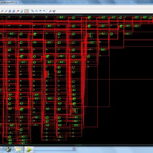
The latest video coding standard high-efficiency video coding (HEVC) provides 50% improvement in coding efficiency compared to H.264/AVC to meet the rising demands for video streaming, better video quality, and higher resolution. The deblocking filter (DF) and sample adaptive offset (SAO) play an important role in the HEVC encoder, and the SAO is newly adopted in HEVC. Due to the high throughput requirement in the video encoder, design challenges such as data dependence, external memory traffic, and on-chip memory area become even more critical. To solve these problems, we first propose an interlacing memory organization on the basis of quarter-LCU to resolve the data dependence between vertical and horizontal filtering of DF. The on-chip SRAM area is also reduced to about 25% on the basis of quarter-LCU scheme without throughput loss. We also propose a simplified bitrate estimation method of rate-distortion cost calculation to reduce the computational complexity in the mode decision of SAO. Our proposed hardware architecture of combined DF and SAO is designed for the HEVC intraencoder, and the proposed simplified bitrate estimation method of SAO can be applied to both intra- and intercoding. As a result, our design can support ultrahigh definition 7680 × 4320 at 40 f/s applications at merely 182 MHz working frequency. Total logic gate count is 103.3 K in 65 nm CMOS process.
List of the following materials will be included with the Downloaded Backup:A Computation and Energy Reduction Technique for HEVC Discrete Cosine Transform
In this paper, a novel computation and energy reduction technique for High Efficiency Video Coding (HEVC) Discrete Cosine Transform (DCT) for all Transform Unit (TU) sizes is proposed. The proposed technique reduces the computational complexity of HEVC DCT significantly at the expense of slight decrease in PSNR and slight increase in bit rate by only calculating several pre-determined low frequency coefficients of TUs and assuming that the remaining coefficients are zero. It reduced the execution time of HEVC HM software encoder up to 12.74%, and it reduced the execution time of DCT operations in HEVC HM software encoder up to 37.27%. In this paper, a low energy HEVC 2D DCT hardware for all TU sizes is also designed and implemented using Verilog HDL. The proposed hardware, in the worst case, can process 53 Ultra HD (7680x4320) video frames per second. The proposed technique reduced the energy consumption of this hardware up to 18.9%. Therefore, it can be used in portable consumer electronics products that require a real-time HEVC encoder. The proposed architecture of this paper analysis the logic size, area and power consumption using Xilinx 14.2.
List of the following materials will be included with the Downloaded Backup:A Deblocking Filter Hardware Architecture for the High Efficiency Video Coding Standard
The new deblocking filter (DF) tool of the next generation High Efficiency Video Coding (HEVC) standard is one of the most time consuming algorithms in video decoding. In order to achieve real-time performance at low-power consumption, we developed a hardware accelerator for this filter. This paper proposes high throughput hardware architecture for HEVC deblocking filter employing hardware reuse to accelerate filtering decision units with a low area cost. Our architecture achieves either higher or equivalent throughput with 5X-6X lower area compared to state of-the-art deblocking filter architectures. The proposed architecture of this paper analysis the logic size, area and power consumption using Xilinx 14.2.
List of the following materials will be included with the Downloaded Backup:A Dual-Mode ECG Segment Export Tool with RGB and Grayscale Hex Encoding in MATLAB
Project Details :
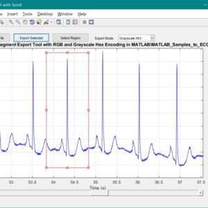
Electrocardiography (ECG) is a vital non-invasive diagnostic technique used to record the electrical activity of the heart. With increasing emphasis on digital healthcare and remote diagnostics, automated and efficient ECG data handling systems are becoming crucial. This work presents a MATLAB-based Graphical User Interface (GUI) framework designed for interactive ECG waveform analysis, segment selection, image generation, and hexadecimal encoding. The system accepts standard ECG data files in .txt format, processes them for visual inspection, and provides an intuitive scrollable interface to examine long-duration signals. A region of interest can be manually selected using a resizable rectangle tool. Upon selection, the user can export the waveform as a clean image (without axis ticks, titles, or grid lines) in a standardized resolution of 256×256 pixels. To accommodate further integration with embedded systems, AI pipelines, or hardware implementations, the application allows users to convert the exported image into either grayscale or RGB hexadecimal representations. The system supports two modes: RGB HEX (outputs R.txt, G.txt, B.txt) and Grayscale HEX (outputs Grayscale.txt), where each pixel’s intensity is encoded in two-digit hexadecimal format. This dual-format capability is controlled via a dropdown menu for easy toggling. The GUI is fully compatible with MATLAB R2018a and includes legacy support by replacing newer functions (such as writematrix) with older equivalents like dlmwrite. The application provides a real-time, interactive ECG visualization platform while also serving as a data preparation tool for machine learning models, microcontroller visualization, and FPGA-based healthcare signal processing. Its ability to convert waveform data into structured visual and hexadecimal forms bridges the gap between clinical signal acquisition and computational processing. This flexible, open-ended tool is particularly beneficial for researchers working in biomedical signal processing, embedded systems, and AI-based ECG classification.
List of the following materials will be included with the Downloaded Backup:A Low Cost and High Throughtput FPGA Implementation of the Retinex Algorithm for Real Time Video Enhancement
Abstract:
For video applications in a special environment such as medical imaging, space exploration, and underwater exploration, the video captured by an image sensor is often deteriorated because of low lighting conditions. Therefore, it is necessary to enhance the part of the image that is too dark to distinguish details while maintaining the remaining part with the same brightness. The retinex algorithm is widely used to restore naturalness of a video, especially exhibiting outstanding performance in the enhancement of a dark area. However, it demands large computational complexity because of its intricate structure, such as the Gaussian filter and exponentiation operations, and consequently, it is difficult to process in real time. This article presents a low-cost and high-throughput design of the retinex video enhancement algorithm. The hardware (HW) design is implemented using a field-programmable gate array (FPGA), and it supports a throughput of 60 frames/s for a 1920 × 1080 image with negligible latency. The proposed FPGA design minimizes HW resources while maintaining the quality and the performance by using a small line buffer instead of a frame buffer, by applying the concept of approximate computing for the complex Gaussian filter, and by designing a new and nontrivial exponentiation operation. The proposed design makes it possible to significantly reduce HW resources (up to 79.22% of total resources) compared to existing systems and is compatible with commercialized devices through the standard HDMI/DVI video ports.
List of the following materials will be included with the Downloaded Backup:A Low Cost FPGA Implementation of Retinex Based Low-Light Image Enhancement Algorithm
Base Paper Abstract:
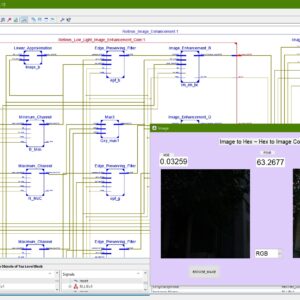
Real-time low-light image enhancement has several potential applications, such as advanced driver assistance systems (ADAS), remote sensing, object tracking, etc. The Retinex-based algorithms are mostly used to restore the visibility of low-light images. However, they perform complex mathematical operations over a large spatial window. Consequently, their hardware realization is tedious, and few researchers have attempted to address this problem. In this brief, we propose a Retinex-based algorithm that employs a low-cost edge-preserving filter for illumination estimation. Although certain approximations are used to curtail the hardware logic resource requirement, the quality of the enhanced image is not compromised. The proposed architecture requires only 10868 LUTs and 7409 registers when implemented on ZynQ 7 FPGA. Moreover, it can process HD images (1920×1080) at the rate of 60 frames per second (fps).
List of the following materials will be included with the Downloaded Backup:A New Parallel VLSI Architecture for Real-time Electrical Capacitance Tomography
This paper presents a fixed-point reconfigurable parallel VLSI hardware architecture for real-time Electrical Capacitance Tomography (ECT). Another FPGA module performs the inverse steps of the tomography algorithm. A dual port built-in memory banks store the sensitivity matrix, the actual value of the capacitances, and the actual image with RGB format. A two dimensional (2D) core multiprocessing elements (PE) engine intercommunicates with these memory banks via parallel buses. We are focus only on the FPGA module because the design is decide the power consumption and cost. The proposed architecture of this paper analysis the logic size, area and power consumption using Xilinx 14.2.
List of the following materials will be included with the Downloaded Backup:A Real-Time FHD Learning Based Super Resolution System Without a Frame Buffer
Abstract:
The main aim of the Single image (SR) super-resolution is to generate (HR) high-resolution images from (LR) low-resolution images. This paper briefly presents a concept of real time super resolution method of FHD based image extended and scaling processor. The super resolution system includes three blocks of operations. The first is a low-frequency interpolation stage, where bicubic interpolation is used for reconstructing the low-frequency parts of HR images. The second stage generates high-frequency patches by choosing the highest related pre-trained regression function according to each HR low frequency patch. In the third stage, with the high-frequency information, the low-frequency image patches are enhanced and overlapped to construct the SR result. These operations for gaining a high-frequency result are applied to the Y-luminance channel only, while the high-resolution Cb and Cr channels are generated by bicubic interpolation. The proposed system generates the output image resolution of 1920 X 1080 (FHD) by the input of 800 X 800 image size. The proposed architecture performs an anchored neighborhood regression algorithm that generates a high-resolution image from a low-resolution image input using only numbers of line buffers. Finally, super resolution technique is implemented in VHDL and Synthesized in the XILINX VERTEX-5 FPGA and shown the comparison for power, area and delay reports.
List of the following materials will be included with the Downloaded Backup:A VLSI Architecture for Watermarking of Gray scale Images using Weighted Median Prediction
Abstract:
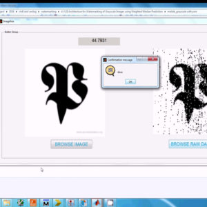
Watermarking the digital data is a familiar technique to authenticate and resolve the copyright issues of multimedia data. This paper proposes a new VLSI architecture for watermarking grayscale images using weighted median prediction operation, as this mechanism will have a minimum computation complexity. In this VLSI based data hiding process the secret digital signature is hidden in the host image and analyzed with the PSNR value and Payload capacity.
List of the following materials will be included with the Downloaded Backup:An Aadhaar-Authenticated FPGA-Based Electronic Voting Machine with EPIC Key Derived
Base paper Abstract:
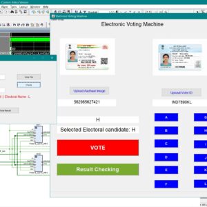
Electronic voting machines are widely used to improve election transparency, reduce manual effort, and provide faster result declaration when compared to traditional paper-based voting systems. The integration of digital platforms further enables ease of access, efficient data handling, and automated vote counting. However, existing electronic voting solutions still face critical challenges such as voter impersonation, data tampering, weak software-based security, and lack of strong hardware-level protection, especially when sensitive voter identity information is involved. Most current systems rely on microcontroller-based architectures, centralized databases, or conventional cryptographic algorithms, which introduce vulnerabilities related to key management, higher computational cost, and limited resistance to physical and logical attacks. To address these issues, this work proposes an Aadhaar-authenticated FPGA-based electronic voting machine with EPIC key–derived lightweight cryptographic vote protection. In the proposed system, Aadhaar number and Voter ID (EPIC) information are captured through a MATLAB-based graphical user interface and securely stored as voter records. The EPIC number is used to derive an 80-bit cryptographic key, while the complete voter information is formatted into a 256-bit data frame and processed within FPGA block memory. Lightweight PRESENT cipher encryption, along with cipher and key shuffling techniques, is employed to protect voter data at the hardware level, ensuring confidentiality and integrity. Decryption is performed using a reverse process to enable authenticated vote verification and result checking without exposing encrypted data. The novelty of this work lies in EPIC key–based dynamic key generation combined with FPGA-based lightweight cryptography, eliminating external key storage and reducing attack surfaces. The system ensures secure authentication, tamper resistance, low resource utilization, and reliable vote verification. Performance and functionality are validated using MATLAB for GUI and data handling, and Verilog HDL for FPGA implementation, demonstrating a secure, efficient, and hardware-trusted electronic voting solution.
List of the following materials will be included with the Downloaded Backup:An Efficient Image Encryption Algorithm Based on Innovative DES Structure and Hyperchaotic Keys
Base Paper Abstract:
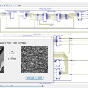
In fact, as a traditional encryption method, DES has been certified as an unsuitable tool for ciphering due to its smaller key space. Further, in concern of the real-time encryption in the current fast communication era, such as 5G, long-time as well as large computational level processes are not gotten into the consideration. As a result, an innovative encryption structure with hyperchaotic keys for efficient encryption is constructed, where the frame of DES structure is applied, the plain image is shuffled through row and column directions in the first round, and then rearranged to be 64 blocks to fit into the frame of DES structure for 4 rounds ciphering with hyperchaotic subkeys. Also, in order to encrypt the content of the image at the block level, a set of alternative S-box has been produced in this article as well. The simulation results indicate that the proposed scheme is feasible and reliable for digital image encrypting, not only a large key space can be obtained, but also the low correlation of the adjacent contents can be achieved, and further, in comparison of several existing approaches, less-computational resource can be proven as well. In particular, due to the innovative DES structure, the computational speed is significantly faster than the original DES algorithm and many other chaos-based image ciphering schemes.
List of the following materials will be included with the Downloaded Backup:An Innovative Area Efficient Pixel Shuffling Method for Image Encryption Algorithm
Proposed Abstract:
In image processing and computer vision, pixel shuffling is a method used to increase an image's resolution without adding more parameters or network complexity. With this technique, a low-quality image's pixels are rearranged to produce an output with a better resolution. Pixel shuffling has proven successful in a number of applications, such as image synthesis, super-resolution, and style transfer. Its simplicity and efficiency make it an attractive option for tasks where increasing image resolution is essential, while avoiding the computational overhead associated with more complex architectures. The image line buffer based pixel shuffling technique presented in this study is an alternative to the classic method, which takes up more logic space in VLSI implementations. This proposed method splits and reconstructs the source photos using a 5x5 image line buffer. With the use of block interleave techniques, this pixel shuffling approach handled row and column sequence using this 5x5 picture line buffer. In conclusion, this study was compared with the PSNR and SSIM value; comparisons of logic sizes for area, latency, and power were also examined.
List of the following materials will be included with the Downloaded Backup:An Ultra-Efficient Approximate Multiplier with Error Compensation for Error-Resilient Applications
Base Paper Abstract:
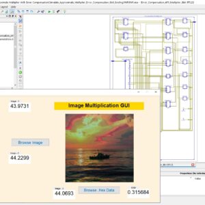
Approximate computing is a promising paradigm for trading off accuracy to improve hardware efficiency in error-resilient applications such as neural networks and image processing. This brief presents an ultra-efficient approximate multiplier with error compensation capability. The proposed multiplier considers the least significant half of the product a constant compensation term. The other half is calculated precisely to provide an ultra-efficient hardware-accuracy tradeoff. Furthermore, a low-complexity but effective error compensation module (ECM) is presented, significantly improving accuracy. The proposed multiplier is simulated using HSPICE with 7nm tri-gate Fin FET technology. The proposed design significantly improves the energy-delay product, on average, by 77% and 54% compared to the exact and existing approximate designs. Moreover, the proposed multiplier’s accuracy and effectiveness in neural networks and image multiplication are evaluated using MATLAB simulations. The results indicate that the proposed multiplier offers high accuracy comparable to the exact multiplier in NNs and provides an average PSNR of more than 51dB in image multiplication. Accordingly, it can be an effective alternative for exact multipliers in practical error-resilient applications.
List of the following materials will be included with the Downloaded Backup:Area and Power Efficient Truncated Booth Multipliers Using Approximate Carry-Based Error Compensation
Base Paper Abstract:
Approximate computing is a promising technique to elevate the performance of digital circuits at the cost of reduced accuracy in numerous error-resilient applications. Multipliers play a key role in many of these applications. In this brief, we propose a truncation based Booth multiplier with a compensation circuit generated by selective modifications in k-map to circumvent the carry appearing from the truncated part. By judicious mapping, hardware pruning and output error reduction is achieved simultaneously. In the quest of power and accuracy trade-off, Truncated and Approximate Carry based Booth Multipliers (TACBM) are proposed with a range of designs based on truncation factor w. When compared with the state-of-the-art multipliers, TACBM outperforms in terms of accuracy and Area Power savings. TACBM (w = 10) provides with 0.02% MRED and 23% reduction in Area-Power product compared to exact Booth multiplier. The multipliers are evaluated using image blending and Multilayer perceptron (MLP) neural network and a high value of accuracy (95.63%) for MLP is achieved.
List of the following materials will be included with the Downloaded Backup:Area-Time Efficient Streaming Architecture for FAST and BRIEF Detector
Abstract:
The combination of FAST corners and BRIEF descriptors provide highly robust image features. We present a novel detector for computing the FAST-BRIEF features from streaming images. To reduce the complexity of the BRIEF descriptor, we employ an optimized adder tree to perform summation by accumulation on streaming pixels for the smoothing operation. Since the window buffer used in existing designs for computing the BRIEF point-pairs are often poorly utilized, we propose an efficient sampling scheme that exploits register reuse to minimize the number of registers. Synthesis results based on 65- nm CMOS technology show that the proposed FAST-BRIEF core achieves over 40% reduction in area-delay product compared to the baseline design. In addition, we show that the proposed architecture can achieve 1.4x higher throughput than the baseline architecture with slightly lower energy consumption.
List of the following materials will be included with the Downloaded Backup:Block Interleaver Design for High Data Rate Wireless Networks
With increasing data rates in wireless communication, quality of service (QoS) has become a major issue. This is more with fading channels transmitting huge volumes of data. QoS is degraded by inter-symbol interference (ISI) and related errors. One of the simplest and convenient techniques to overcome such errors is interleaving, which is used efficiently in wireless applications. It has found applications for combating burst errors that creeps up in the channel during transmission. In this paper, an efficient model of a block interleaver using a hardware description language (Verilog) is proposed. The proposed technique reduces consumption of FPGA resources to a large extent, which implies low power consumption. The proposed architecture of this paper analysis the logic size, area and power consumption using Xilinx 14.2.
List of the following materials will be included with the Downloaded Backup:Constant Time Hardware Architecture for a Gaussian Smoothing Filter
Abstract:
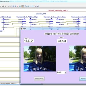
In this paper a new and highly efficient hardware architecture for a bit-serial implementation of a 3*3 filter on FPGA is developed and presented. The concept is implemented on a Gaussian blur spatial filter and it can be extended to other filters with similar characteristics. The proposed Single Instruction Multiple Data (SIMD) architecture provides a constant operating time independent of the size of the given image while the arithmetic operations are limited to the operations of addition. The Multiple Instruction Multiple Data (MIMD) performance is achieved in a near fraction of the cost. Thus, the hardware’s utilization is optimized. The total time needed to perform the filter of interest on the given image is solely dependent on the working clock frequency. The proposed design is evaluated using a small image and is implemented on two FPGA families with various sizes of an image. Also, it is compared with other architectures.
List of the following materials will be included with the Downloaded Backup:Design and Analysis of Approximate Compressors for Multiplication
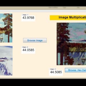
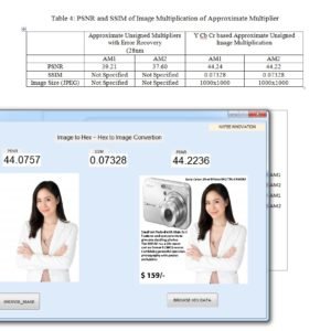
Inexact computing is particularly interesting for computer arithmetic designs. Implementation of 8X8 truncated multipliers using Very High Speed Integrated Circuit Hardware Description Language (VHDL). Truncated multipliers can be used in the image multiplication application. This multiplier is automatically truncating the output and reduces the power consumption and are comparing to other multipliers. The proposed architecture of this paper analysis the logic size, area and power consumption using Xilinx 14.2.
List of the following materials will be included with the Downloaded Backup:Design and Implementation of Efficient Streaming Deblocking and SAO Filter for HEVC Decoder
We have also Code for 720 x 576 Image Resolution using 64 x 64 Block Size of HEVC. Cost of this Update work in High Resolution Rs. 45,000/- ( Rs. 45,000/- + Rs. 35,000/- ) : Total Cost : Rs. 80,000/-
Abstract:
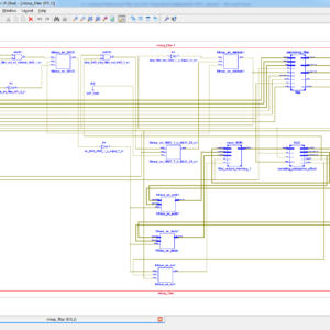
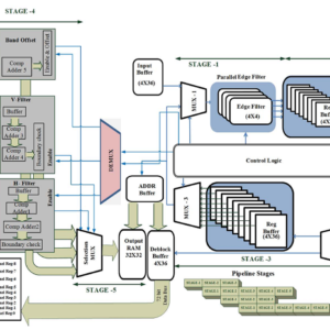
This paper aims to design an efficient mixed serial five-stage pipeline processing hardware architecture of deblocking filter (DBF) and sample adaptive offset (SAO) filter for high efficiency video coding decoder. The proposed hardware is designed to increase the throughput and reduce the number of clock cycles by processing the pixels in a stream of 4 × 36 samples in which edge filters are applied vertically in a parallel fashion for processing of luma/chroma samples. Subsequently these filtered pixels are transposed and reprocessed through vertical filter for horizontal filtering in a pipeline fashion. Finally, the filtered block transposed back to the original orientation and forwarded to a three-stage pipeline SAO filter. The proposed architecture is implemented in field programmable gate array and application specific integrated circuit platform using 90-nm library. Experimental results illustrate that the proposed DBF and SAO architecture decreases the processing cycles (172) required for processing each 64 × 64 or large coding unit compared with the state-of-the-art literature with the increase of gate count (593.32K) including memory. The results show that the throughput of the proposed filter can successfully decode ultrahigh definition video sequences at 200 frames/s at 341 MHz.
List of the following materials will be included with the Downloaded Backup:Design of Power and Area Efficient Approximate Multipliers
Abstract:
Approximate computing can decrease the design complexity with an increase in performance and power efficiency for error resilient applications. This brief deals with a new design approach for approximation of multipliers. The partial products of the multiplier are altered to introduce varying probability terms. Logic complexity of approximation is varied for the accumulation of altered partial products based on their probability. The proposed approximation is utilized in two variants of 16-bit multipliers. Synthesis results reveal that two proposed multipliers achieve power savings of 72% and 38%, respectively, compared to an exact multiplier. They have better precision when compared to existing approximate multipliers. Mean relative error figures are as low as 7.6% and 0.02% for the proposed approximate multipliers, which are better than the previous works. Performance of the proposed multipliers is evaluated with an image processing application, where one of the proposed models achieves the highest peak signal to noise ratio.
List of the following materials will be included with the Downloaded Backup:Design of ultra-low power consumption approximate 4-2 compressors based on the compensation characteristic
Abstract:
Approximate computing is tentatively applied in some digital signal processing applications which have an inherent tolerance for erroneous computing results. The approximate arithmetic blocks are utilized in them to improve the electrical performance of these circuits. Multiplier is one of the fundamental units in computer arithmetic blocks. Moreover, the 4-2 compressors are widely employed in the parallel multipliers to accelerate the compression process of partial products. In this paper, three novel approximate 4-2 compressors are proposed and utilized in 8-bit multipliers. Meanwhile, an error-correcting module (ECM) is presented to promote the error performance of approximate multiplier with the proposed 4-2 compressors. In this paper, the number of the approximate 4-2 compressor’s outputs is innovatively reduced to one, which brings further improvements in the energy efficiency. Compared with the exact 4-2 compressors, the simulation results indicate that the proposed approximate compressors UCAC1, UCAC2, UCAC3 achieve 24.76%, 51.43%, and 66.67% reduction in delay, 71.76%, 83.06%, and 93.28% reduction in power and 54.02%, 79.32%, and 93.10% reduction in area, respectively. And the utilization of these proposed compressors in 8-bit multipliers brings 49.29% reduction of power consumption on average.
List of the following materials will be included with the Downloaded Backup:Dual Quality 4:2 Compressor for Utilizing in Dynamic Accuracy Configurable Multipliers
Abstract:
In this paper, we propose four 4:2 compressors, which have the flexibility of switching between the exact and approximate operating modes. In the approximate mode, these dual-quality compressors provide higher speeds and lower power consumptions at the cost of lower accuracy. Each of these compressors has its own level of accuracy in the approximate mode as well as different delays and power dissipations in the approximate and exact modes. Using these compressors in the structures of parallel multipliers provides configurable multipliers whose accuracies (as well as their powers and speeds) may change dynamically during the runtime. The proposed multiplier saves few adder circuits in partial products, and this proposed multiplier is evaluated with an image processing application. In existing thing, to using this multiplier to design image processing evaluation on only luminance based application, but here the proposed work is modified with Gaussian noise reduction with luminance and chrominance based application, this design to implemented in VHDL, and synthesized in Xilinx S6LX9 FPGA and shown the power, area and delay reports.
List of the following materials will be included with the Downloaded Backup:Efficient Super Resolution Algorithm using Overlapping Bi-cubic Interpolation
Abstract:
In practical CCTV applications, there are problems of the camera with low resolution, camera fields of view, and lighting environments. These could degrade the image quality and it is difficult to extract useful information for further processing. Super-resolution techniques have been proposed widely by the researchers. However, many approaches are complex and are difficult to use in practical scenarios. In this paper, we propose an efficient Super-resolution algorithm using overlapping bi-cubic for hardware implementation. Experimental results are verified using processing time and reconstructed images that can be used in real time applications.
List of the following materials will be included with the Downloaded Backup:Energy-Efficient Approximate Multiplier Design using Bit Significance-Driven Logic Compression
Abstract:
Approximate arithmetic has recently emerged as a promising paradigm for many imprecision-tolerant applications. It can offer substantial reductions in circuit complexity, delay and energy consumption by relaxing accuracy requirements. In this paper, we propose a novel energy-efficient approximate multiplier design using a significance-driven logic compression (SDLC) approach. Fundamental to this approach is an algorithmic and configurable lossy compression of the partial product rows based on their progressive bit significance. This is followed by the commutative remapping of the resulting product terms to reduce the number of product rows. As such, the complexity of the multiplier in terms of logic cell counts and lengths of critical paths is drastically reduced. A number of multipliers with different bit-widths (4-bit to 128-bit) are designed in System Verilog and synthesized using Synopsys Design Compiler. Post-synthesis experiments showed that up to an order of magnitude energy savings, and reductions of 65% in critical delay and almost 45% in silicon area can be achieved for a 128-bit multiplier compared to an accurate equivalent. These gains are achieved with low accuracy losses estimated at less than 0.00071 mean relative error. Additionally, we demonstrate the energy-accuracy trade-offs for different degrees of compression, achieved through configurable logic clustering. In evaluating the effectiveness of our approach, a case study image processing application showed up to 68.3% energy reduction with negligible losses in image quality expressed as peak signal-to-noise ratio (PSNR).
List of the following materials will be included with the Downloaded Backup:Floating-point discrete wavelet transform-based image compression on FPGA
Abstract:
In the era of data transmission through internet, image compression is considered an active research topic, decreasing the amount of data storage for faster data transfer. In this paper, the hardware implementation of an image compression system using Discrete Wavelet Transform (DWT) is presented. The transposed form Finite Impulse Response (FIR) filter is employed for performing the convolution process, on which the DWT is based. The design is generic to fit for different wavelet types and symmetric to expand for filters of multiple taps. The architecture is implemented on FPGA using IEEE-754 single precision. Floating-Point representation offered higher precision and better accuracy compared to scaled integer values. The proposed hardware design is implemented on Virtex 5 FPGA achieving 243.6 MHz clock frequency.
List of the following materials will be included with the Downloaded Backup:FPGA Implementation of Image Line Buffer to Split and reconstruct a 3×3 size of image pixel with using FIFO Design
Proposed Abstract:
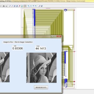
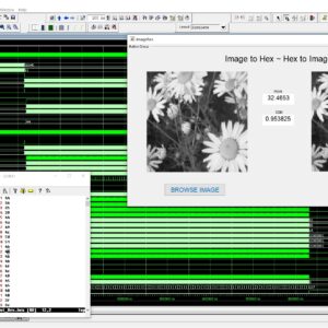
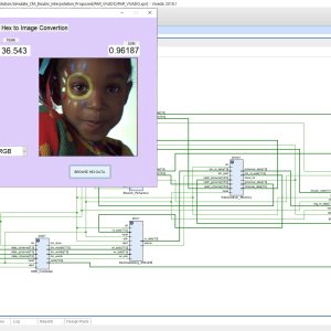
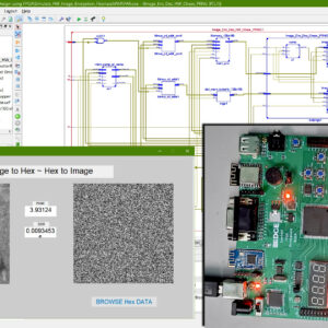
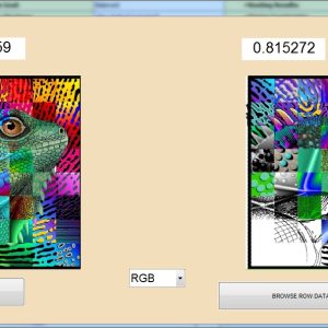
Image line buffers are used in several kinds of image processing applications, particularly where operations must be executed on a per-line basis in order to optimize efficiency. There are many typical applications associated with this technology, including real-time video processing, image filtering, edge detection, computer vision, memory optimization, parallel processing, compression algorithms, and medical imaging. In the context of image and video processing applications, the use of image line buffers may contribute to the optimization of operations when dealing with a continuous stream of frames processed in real time. In the context of image processing, convolutional processes are often used for tasks like as image filtering and blurring. These operations are typically carried out on a per-pixel basis, wherein the value assigned to each pixel is determined by the values of its adjacent pixels. The proposed structure was created using a First-In-First-Out (FIFO) based approach, aiming to decrease the number of logic sizes and complexity in Very Large Scale Integration (VLSI) design architecture. The conversion of design images to hexadecimal and hexadecimal to image format is accomplished using MATLAB GUI applications. These applications also facilitate the comparison of Peak Signal-to-Noise Ratio (PSNR) and Structural Similarity Index Measure (SSIM) values. The internal architecture of the system is implemented using Verilog Hardware Description Language (HDL). Additionally, the simulation is conducted using Modelsim. Furthermore, the system's performance parameters, including area, delay, and power consumption, are compared with those of the Xilinx Vertex-5 Field Programmable Gate Array (FPGA).
List of the following materials will be included with the Downloaded Backup:FPGA implementation of low power and high speed image edge detection algorithm
Abstract:
Image processing is a vital task in data processing system for applications in medical fields, remote sensing, microscopic imaging etc., Algorithms for processing image exist except for real time system style, hardware implementation is most popular principally. This paper presents a design for Sobel filter based edge detection on Field Programmable Gate Array (FPGA) board. Hardware implementation of the Sobel edge detection algorithm is chosen because it presents an honest scope for similarity over software package. On the opposite hand, Sobel edge detection will work with less deterioration in high level of noise. Edges are primarily the noticeable variation of intensities in a picture. Edges facilitate to spot the placement of an object and also the boundary of a selected entity within the image. It conjointly helps in feature extraction and pattern recognition. Hence, edge detection is of nice importance in pc vision. The planned design for edge detection exploitation Sobel algorithm is designed using structural Verilog lipoprotein synthesized exploitation Cadence Genus and enforced using Cadence Innovus. The practicality of the planning is verified exploitation normal pictures by FPGA implementation. The proposed architecture reduce the power, delay and space complexity compare to three existing architectures.
List of the following materials will be included with the Downloaded Backup:FPGA Implementation of TFT 1.8 inch SPI 128×160 Display ROM Interface
Simple Description:
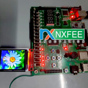
This ST7735R is a display controller used in small TFT (Thin-Film Transistor) LCD displays. It is often used in combination with microcontrollers or FPGAs to drive these displays. The controller supports the Serial Peripheral Interface mode of communication for sending commands and data to the display. This TFT display helps with a greater number of image and video processing applications. Here we have implemented this TFT display in FPGA hardware implementation using Verilog HDL with a novelty-based architecture design. Finally shown the output with TFT Display.
List of the following materials will be included with the Downloaded Backup:FPGA-Based Brain Tumor Detection from MRI Using 3×3 Convolution Soft IP Core with Stride 1
Base Paper Abstract:
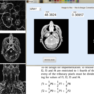
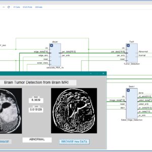
This paper presents an efficient FPGA-based system for automatic brain tumor detection from MRI images using a 3x3 convolutional edge detection method with stride 1. The proposed architecture is developed as a soft IP core in Verilog HDL and synthesized on a Xilinx Zynq 7000 FPGA platform. The system applies a customized 3x3 convolution kernel over each MRI image with stride 1, ensuring that every pixel is processed and fine image details are preserved for accurate tumor detection. Edge detection results are used to segment and highlight abnormal regions, and a thresholding mechanism is employed to differentiate between normal and abnormal images. Hardware resource utilization—including look-up tables (LUTs), flip-flops (FFs), and power consumption—is analyzed after synthesis to verify system efficiency. Experimental results confirm that the proposed FPGA implementation provides real-time processing and reliable brain tumor detection with low power usage, making it suitable for portable and embedded medical devices. The stride 1 approach guarantees maximum detection accuracy and detailed edge representation in all test cases.
List of the following materials will be included with the Downloaded Backup:Fully Pipelined Low-Cost and High-Quality Color Demosaicking VLSI Design for Real-Time Video Applications
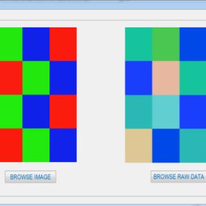
This system presents a fully pipelined color demosaicking design. To improve the quality of reconstructed images, a linear deviation compensation scheme was created to increase the correlation between the interpolated and neighboring pixels. Furthermore, immediately interpolated green color pixels are first to be used in hardware-oriented color demosaicking algorithms, which efficiently promoted the quality of the reconstructed image. A boundary detector and boundary mirror machine were added to improve the quality of pixels located in boundaries. In addition, a hardware sharing technique was used to reduce the hardware costs of three interpolators. Finally these are implemented and get the simulated result is compared to the previous architecture. The code are simulated and power, area, cost are taken using Xilinx 14.2 software and MATLAB. Compared with the previous low complexity designs, this work has the benefits in terms of low cost, low power consumption, and high performance.
List of the following materials will be included with the Downloaded Backup:
Hardware Architecture for Adaptive Edge Directed Interpolation Algorithm
Base Paper Abstract:
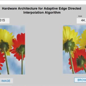
Demosaicking refers to the reconstruction of full color image by the incomplete color samples produced by the single-chip image sensor. So there is a need of interpolation to obtain the missing color pixels. In this work a hardware architecture has been proposed for the adaptive edge-directed interpolation algorithm which uses an edge estimator for the interpolation. The proposed hardware architecture is implemented in Verilog HDL (Hardware Description Language) and synthesized using Cadence Genus compiler with 90nm technology in typical mode. For the proposed architecture, the power dissipation is found to be 26 mW, delay is 7.2 ns and requires 2.3 mm2 area. The demosaicked images obtained using the proposed architecture is observed to have better image quality in terms of peak signal-to-noise ratio and structural similarity while comparing with existing architectures.
List of the following materials will be included with the Downloaded Backup:Hardware-Optimized High-Quality Super-Resolution Accelerator for Real-Time Edge Computing
Base Paper Abstract:
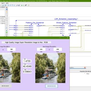
Super-resolution (SR) techniques have been employed to construct high-definition images from low-quality images. Various neural networks have demonstrated excellent image-reconstruction quality in SR accelerators. However, deploying SR networks on edge devices is limited by resources and power consumption induced by significant algorithm parameters, computation complexity, and external memory accesses. This work explores the hardware algorithm co-design techniques to provide an end-to-end platform with a lightweight super-resolution network (LSR) and an efficient, high-quality SR accelerator HDSuper. For algorithm design, the improved depth-wise separable convolution and pixel shuffle layers are developed to reduce network size and computation complexity by considering the hardware constraints. Also, the improved channel attention (CA) blocks enhance the image reconstruction quality. For hardware accelerator design, we design a unified computing core (UCC) combined with an efficient flattening-and allocation (F-A) mapping strategy to support various operators with high computational utilization. In addition, we design the patch computing scheme to reduce the external memory access of the hardware architecture. Based on the evaluation, the proposed algorithm achieves high-quality image reconstruction with 37.44d B PSNR. Finally, the FPGA demonstration and ASIC layout under UMC 55nm are achieved with low power consumption (2.08 W and 152mW) under the lowest hardware resources compared to the state-of-the-art works.
List of the following materials will be included with the Downloaded Backup:Image Demosaicking using Super Resolution Techniques
Base Paper Abstract:
Limitations do exist on capturing the full color information in a scene, apart from the resolution of captured images. Therefore, mosaic images are the preferred format in digital cameras, where incomplete set of color information is acquired. In this paper, a super resolution demosaicking (SRD) approach is proposed to reconstruct an enhanced-resolution full-color image from the observed samples, robustly and without the need for a training process. The acquisition model assumes degraded observations using known blur and noise. The reconstruction approach iteratively estimates the unknown registration parameters and the demosaicking image simultaneously. Qualitative and quantitative experiments performed on synthetic observations reveal high performance images.
List of the following materials will be included with the Downloaded Backup:Image Encryption on FPGA Using Chaotic PRNG and LFSR: TFT Display Integration
Proposed Abstract:
Image encryption plays a crucial role in securing digital communication, especially with the rise of cyber threats and data breaches. This research focuses on implementing a Chaos-based Pseudorandom Number Generator (PRNG) for image encryption and compares its performance with Fibonacci and Galois-based Linear Feedback Shift Registers (LFSRs). The proposed system is developed using Verilog HDL and synthesized on a Xilinx Spartan-6 FPGA, with a real-time TFT display interface for encrypted and decrypted image visualization. Traditional LFSR-based PRNGs are widely used due to their simplicity and speed; however, they suffer from predictable periodicity and lower security strength. In contrast, Chaos-based PRNGs provide higher randomness and security, making them ideal for cryptographic applications. In this work, different PRNG approaches are analyzed based on randomness quality using the NIST test suite, hardware resource utilization (LUTs, FFs, power consumption), and encryption security (correlation, entropy, and key sensitivity). The Chaos-based PRNG is then integrated into a stream cipher encryption system, where image pixels are transformed using bitwise XOR and chaotic substitution-permutation operations. The encrypted images are decrypted using the inverse transformation and displayed on a TFT display, ensuring real-time validation. Experimental results confirm that the Chaos-based PRNG outperforms LFSR-based PRNGs in security strength and randomness, while maintaining efficient FPGA resource utilization. This work demonstrates a practical hardware-based image encryption system, suitable for real-time, secure multimedia applications such as IoT, medical imaging, and defense systems. Future enhancements include optimizing chaos-based PRNGs for high-speed cryptographic applications and exploring AI-based encryption techniques for enhanced security.
List of the following materials will be included with the Downloaded Backup:JF-Cut: A Parallel Graph Cut Approach for Large-Scale Image and Video
Graph cut has proven to be an effective scheme to solve a wide variety of segmentation problems in vision and graphics community. The main limitation of conventional graph-cut implementations is that they can hardly handle large images or videos because of high computational complexity. Even though there are some parallelization solutions, they commonly suffer from the problems of low parallelism (on CPU) or low convergence speed (on GPU). In this paper, we present a novel graph-cut algorithm that leverages a parallelized jump flooding technique and an heuristic push-relabel scheme to enhance the graph-cut process, namely, back-and-forth relabel, convergence detection, and block-wise push-relabel. The entire process is parallelizable on GPU, and outperforms the existing GPU-based implementations in terms of global convergence, information propagation, and performance. We design an intuitive user interface for specifying interested regions in cases of occlusions when handling video sequences. Experiments on a variety of data sets, including images (up to 15 K×10 K), videos (up to 2.5K×1.5K×50), and volumetric data, achieve highquality results and a maximum 40-fold (139-fold) speedup over conventional GPU (CPU-)-based approaches.
List of the following materials will be included with the Downloaded Backup:Low Power FPGA Design Using Memoization Based Approximate Computing
Field-programmable gate arrays (FPGAs) are increasingly used as the computing platform for fast and energy efficient execution of recognition, mining, and search applications. Approximate computing is one promising method for achieving energy efficiency. Compared with most prior works on approximate computing, which target approximate processors and arithmetic blocks, this paper presents an approximate computing methodology for FPGA-based design. It studies memoization as a method for approximation on FPGA and analyzes different architectural and design parameters that should be considered. The proposed design flow leverages on high-level synthesis to enable memoization-based microarchitecture generation, thus also facilitating a C-to-register-transfer-level synthesis. When compared with the previous approaches of bit-width truncation and approximate multipliers, memoization-based approximate computation on FPGA achieves a significant dynamic power saving (around 20%) with very small area overhead (<5%) and better power-to-signal noise ratio values for the studied image processing benchmarks. The proposed architecture of this paper is verified using vivado HLS..
List of the following materials will be included with the Downloaded Backup:
Low-Power Approximate Unsigned Multipliers with Configurable Error Recovery
Abstract:
Approximate circuits have been considered for applications that can tolerate some loss of accuracy with improved performance and/or energy efficiency. Multipliers are key arithmetic circuits in many of these applications including digital signal processing (DSP). In this paper, a novel approximate multiplier with a low power consumption and a short critical path is proposed for high-performance DSP applications. This multiplier leverages a newly designed approximate adder that limits its carry propagation to the nearest neighbors for fast partial product accumulation. Different levels of accuracy can be achieved by using either OR gates or the proposed approximate adder in a configurable error recovery. The multipliers using these two error reduction strategies are referred to as approximate multiplier 1 (AM1) and approximate multiplier 2 (AM2), respectively. Both AM1 and AM2 have a low mean error distance, i.e., most of the errors are not significant in magnitude. Compared to a Wallace multiplier optimized for speed, an 8×8 AM1 with 4 MSBs (most significant bits) for error reduction and synthesized using a 28 nm CMOS process shows a 60% reduction in delay (when optimized for delay) and a 42% reduction in power dissipation (when optimized for area). In a 16×16 design, half of the least significant partial products are truncated for AM1 and AM2, which are thus denoted as TAM1 and TAM2, respectively. Compared with the Wallace multiplier, TAM1 and TAM2 save from 50% to 66% in power, when optimized for area. Compared to existing approximate multipliers, AM1, AM2, TAM1 and TAM2 show significant advantages in accuracy with a high performance. AM2 has a better accuracy compared to AM1 but with a longer delay and higher power consumption. Image processing applications including image sharpening and smoothing are considered to show the quality of the approximate multipliers in error-tolerant applications. By utilizing an appropriate error recovery, the proposed approximate multipliers achieve similar processing accuracy as traditional exact multipliers, but with significant improvements in power.
List of the following materials will be included with the Downloaded Backup:VLSI Implementation of an Edge-Oriented Image Scaling Processor
Abstract:
Image scaling is a very important technique and has been widely used in many image processing applications. In this paper, we present an edge-oriented area-pixel scaling processor. To achieve the goal of low cost, the area-pixel scaling technique is implemented with a low-complexity VLSI architecture in our design. A simple edge catching technique is adopted to preserve the image edge features effectively so as to achieve better image quality. Compared with the previous low-complexity techniques, our method performs better in terms of both quantitative evaluation and visual quality. The seven-stage VLSI architecture of our image scaling processor contains 10.4-K gate counts and yields a processing rate of about 200 MHz by using TSMC 0.18- m technology.
List of the following materials will be included with the Downloaded Backup:VLSI Implementation of Efficient Image Watermarking Algorithm
Abstract:
The watermarking is the important multimedia content for authentication and security in nowadays. We are proposed to implement the watermarking in FPGA with VLSI architecture. And also use the Haar discrete wallet transform and bit plane slicing for creating the water marking images and extracted watermark images. The area, power, delay of the proposed architecture is analysis using Xilinx 14.2.
List of the following materials will be included with the Downloaded Backup:VLSI-Oriented Lossy Image Compression Approach using DA-Based 2D-Discrete Wavelet
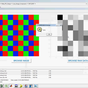
We introduced a Discrete Wavelet Transform (DWT) based VLSI-oriented lossy image compression approach, widely used as the core of digital image compression. Here, Distributed Arithmetic (DA) technique is applied to determine the wavelet coefficients, so that the number of arithmetic operation can be reduced substantially. As well, the compression rate is enhanced with the aid of introducing RW block that blocks some of the coefficients obtained from the high pass filter to zero. Subsequently, Differential Pulse-Code Modulation (DPCM) and huffman-encoding are applied to acquire the binary sequence of the image. The proposed architecture of this paper analysis the logic size, area and power consumption using Xilinx 14.2.
List of the following materials will be included with the Downloaded Backup:Provide Wordlwide Online Support
We can provide Online Support Wordlwide, with proper execution, explanation and additionally provide explanation video file for execution and explanations.
24/7 Support Center
NXFEE, will Provide on 24x7 Online Support, You can call or text at +91 9789443203, or email us nxfee.innovation@gmail.com
Terms & Conditions:
Customer are advice to watch the project video file output, and before the payment to test the requirement, correction will be applicable.
After payment, if any correction in the Project is accepted, but requirement changes is applicable with updated charges based upon the requirement.
After payment the student having doubts, correction, software error, hardware errors, coding doubts are accepted.
Online support will not be given more than 3 times.
On first time explanation we can provide completely with video file support, other 2 we can provide doubt clarifications only.
If any Issue on Software license / System Error we can support and rectify that within end of day.
Extra Charges For duplicate bill copy. Bill must be paid in full, No part payment will be accepted.
After payment, to must send the payment receipt to our email id.
Powered by NXFEE INNOVATION, Pondicherry.
Call us today at : +91 9789443203 or Email us at nxfee.innovation@gmail.com
NXFEE Development & Services

Product Categories
- 2014 (11)
- 2015 (39)
- 2016 (30)
- 2017 (16)
- 2018 (17)
- 2019 (42)
- 2020 (29)
- 2021 (17)
- 2022 (23)
- Accessories (47)
- Area Efficient (117)
- High speed VLSI Design (57)
- IEEE (15)
- Image Processing (40)
- Low power VLSI Design (99)
- NOC VLSI Design (2)
- VLSI (253)
- VLSI 2023 (21)
- VLSI 2024 (18)
- VLSI 2025 (33)
- VLSI 2026 (4)
- VLSI Application / Interface and Mini Projects (31)
- VLSI_2023 (15)
Filter by price
Product Status
Sort by producents

Copyright © 2026 Nxfee Innovation.

