IEEE Transactions on VLSI 2019
Following Novelty based Research Projects not yet Published in Any Journal
Customization Available for Journal Publications
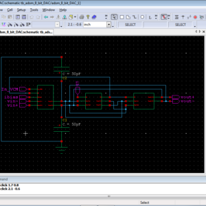
A 0.3-V 37-nW 53-dB SNDR Asynchronous Delta–Sigma Modulator in 0.18-μm CMOS
Abstract:
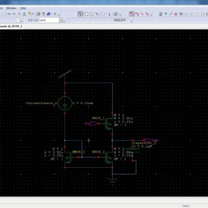
A new solution for an ultralow-voltage bulk driven (BD) asynchronous delta–sigma modulator is described in this paper. While implemented in a standard 0.18-µm CMOS process from the Taiwan Semiconductor Manufacturing Company and supplied with VDD = 0.3 V, the circuit offers a 53.3-dB signal-to-noise and distortion ratio, which corresponds to 8.56-bit resolution. In addition, the total power consumption is 37 nW, the signal bandwidth is 62 Hz, and the resulting power efficiency is 0.79 pJ/conversion. The above-mentioned features have been achieved employing a highly linear transconductor and a hysteretic comparator based on nontailed BD differential pair.
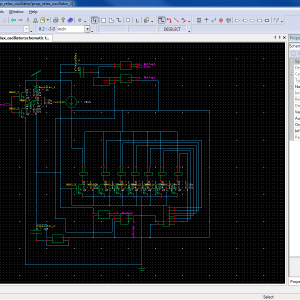
List of the following materials will be included with the Downloaded Backup:A 13.4-MHz Relaxation Oscillator With Temperature Compensation
Abstract:
A low-phase-noise relaxation oscillator uses a digital compensation loop to reduce its temperature coefficient (TC). This relaxation oscillator is fabricated in the 0.18-µm CMOS process. The measured average oscillation frequency is 13.4 MHz. The whole oscillator consumes 157.8 µW under a 1.2-V supply. The measured average TCs of the oscillation frequency with and without compensation are 193.15 and 1098.7 ppm/◦C, respectively. The TC achieves an improvement of 5.7 times. The measured frequency variation is within ±2% from −20 ◦C to 100 ◦C by using the digital compensation loop. The measured phase noise at 100-kHz offset frequency is −104.82 dBc/Hz, and the measured figure of merit (FOM) is −154.4 dBc/Hz
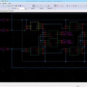
List of the following materials will be included with the Downloaded Backup:A 16-bit 2.0-ps Resolution Two-Step TDC in 0.18-μm CMOS Utilizing Pulse-Shrinking Fine Stage
Abstract:
This paper proposes a time-to-digital converter (TDC) that achieves wide input range and fine time resolution at the same time. The proposed TDC utilizes pulse-shrinking (PS) scheme in the second stage for a fine resolution and two-step (TS) architecture for a wide range. The proposed PS TDC prevents an undesirable non-uniform shrinking rate issue in the conventional PS TDCs by utilizing a built-in offset pulse and an offset pulse width detection schemes. With several techniques, including a built-in coarse gain calibration mechanism, the proposed TS architecture overcomes a nonlinearity due to the signal propagation and gain mismatch between coarse and fine stages. The simulation results of the TDC implemented in a 0.18-µm standard CMOS technology demonstrate 2.0-ps resolution and 16-bit range that corresponds to ∼130-ns input time interval with 0.08-mm2 area. It operates at 3.3 MS/s with 18.0 mW from 1.8-V supply and achieves 1.44-ps single-shot precision. Index Terms— Built-in calibration, pulse shrinking (PS), time-to-digital conversion, two step (TS).
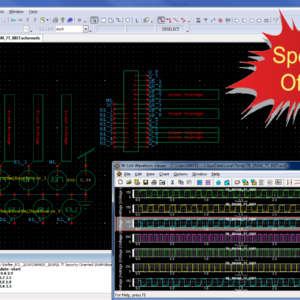
List of the following materials will be included with the Downloaded Backup:A 7T Security Oriented SRAM Bitcell
Abstract:
Power analysis (PA) attacks have become a serious threat to security systems by enabling secret data extraction through the analysis of the current consumed by the power supply of the system. Embedded memories, often implemented with six-transistor (6T) static random access memory (SRAM) cells, serve as a key component in many of these systems. However, conventional SRAM cells are prone to side-channel power analysis attacks due to the correlation between their current characteristics and written data. To provide resiliency to these types of attacks, we propose a security-oriented 7T SRAM cell, which incorporates an additional transistor to the original 6T SRAM implementation and a two-phase write operation, which significantly reduces the correlation between the stored data and the power consumption during write operations. The proposed 7T SRAM cell was implemented in a 28 nm technology and demonstrates over 1000× lower write energy standard deviation between write ‘1’ and ‘0’ operations compared to a conventional 6T SRAM. In addition, the proposed cell has a 39%–53% write energy reduction and a 19%–38% reduced write delay compared to other power analysis resistant SRAM cells.
List of the following materials will be included with the Downloaded Backup:A Decoder for Short BCH Codes With High Decoding Efficiency and Low Power for Emerging Memories
Abstract:
In this paper, a double-error-correcting and triple error-detecting (DEC-TED) Bose–Chaudhuri–Hocquenghem (BCH) code decoder with high decoding efficiency and low power for error correction in emerging memories is presented. To increase the decoding efficiency, we propose an adaptive error correction technique for the DEC-TED BCH code that detects the number of errors in a codeword immediately after syndrome generation and applies a different error correction algorithm depending on the error conditions. With the adaptive error correction technique, the average decoding latency and power consumption are significantly reduced owing to the increased decoding efficiency. To further reduce the power consumption, an invalid-transition-inhibition technique is proposed to remove the invalid transitions caused by glitches of syndrome vectors in the error-finding block. Synthesis results with an industry-compatible 65-nm technology library show that the proposed decoders for the (79, 64, 6) BCH code take only 37%–48% average decoding latency and achieve more than 70% power reduction compared to the conventional fully parallel decoder under the 10−4–10−2 raw bit-error rate.
List of the following materials will be included with the Downloaded Backup:A High-Throughput Hardware Accelerator for Lossless Compression of a DDR4 Command Trace
Abstract:
In a memory system, understanding how the host is stressing the memory is important to improve memory performance. Accordingly, the need for the analysis of memory command trace, which the memory controller sends to the dynamic random access memory, has increased. However, the size of this trace is very large; consequently, a high-throughput hardware (HW) accelerator that can efficiently compress these data in real time is required. This paper proposes a high throughput HW accelerator for lossless compression of the command trace. The proposed HW is designed in a pipeline structure to process Huffman tree generation, encoding, and stream merge. To avoid the HW cost increase owing to high throughput processing, a Huffman tree is efficiently implemented by utilizing static random access memory-based queues and bitmaps. In addition, variable length stream merge is performed at a very low cost by reducing the HW wire width using the mathematical properties of Huffman coding and processing the metadata and the Huffman codeword using FIFO separately. Furthermore, to improve the compression efficiency of the DDR4 memory command, the proposed design includes two preprocessing operations, the “don’t care bits override” and the “bits arrange,” which utilize the operating characteristics of DDR4 memory. The proposed compression architecture with such preprocessing operations achieves a high throughput of 8 GB/s with a compression ratio of 40.13% on average. Moreover, the total HW resource per throughput of the proposed architecture is superior to the previous implementations.
List of the following materials will be included with the Downloaded Backup:A Low Complexity I/Q Imbalance Calibration Method for Quadrature Modulator
Abstract:
This brief presents a low-complexity I/Q (in-phase and quadrature components) imbalance calibration method for the transmitter using quadrature modulation. Impairments in analog quadrature modulator have a deleterious effect on the signal fidelity. Among the critical impairments, I/Q imbalance (gain and phase mismatches) deteriorates the residual sideband performance of the analog quadrature modulator degrading the error vector magnitude. Based on the theoretical mismatch analysis of the quadrature modulator, we propose a low-complexity I/Q imbalance extraction algorithm. After the parameter extraction, the transmitter is calibrated by imposing the counter imbalanced mismatch of the transmitter through the digital baseband. In comparison with existing I/Q imbalance calibration methods, the novelty of the proposed method lies in that: 1) only three spectrum measurements of the device-under-test are needed for extraction and calibration of gain and phase mismatches; 2) due to the blind nature of the calibration algorithm, the proposed approach can be readily applicable to an existing I/Q transmitter; 3) no extra hardware that degrades the calibration accuracy is required; and 4) due to the non-iterative nature, the proposed method is faster and computationally more efficient than previously published methods.
List of the following materials will be included with the Downloaded Backup:A Nanopower Biopotential Lowpass Filter Using Subthreshold Current-Reuse Biquads With Bulk Effect Self-Neutralization
Abstract:
A nanopower CMOS 4th-order lowpass filter suitable for biomedical applications is presented. The filter is formed by cascading two types of subthreshold current-reuse biquadratic cell. Each proposed cell is capable of neutralizing the bulk effect that induces the passband attenuation. The nearly 0-dB passband gain can thus be maintained, while the entire filter circuit remains compact and power-efficient. Designed for electrocardiogram detection as an example of application, the filter prototype has been fabricated in a 0.35 µm CMOS process occupying 269 µm × 383 µm chip area. Measurements verify that the filter can operate from a 1.5-V single supply and consumes 5.25 nW, while providing a cutoff frequency of 100 Hz and input-referred noise of 39.38 µVrms. The intermodulation-free dynamic range of 51.48 dB is obtained from a two-tone test of 50 and 60 Hz input frequencies. Compared with state-of-the-art nanopower lowpass filters using the most relevant and reasonable figure of merit, the proposed filter ranks the best.
List of the following materials will be included with the Downloaded Backup:A Novel Design of Flip-Flop Circuits using Quantum Dot Cellular Automata (QCA)
Abstract:
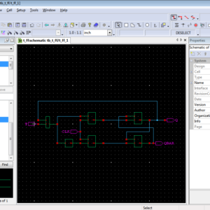
As the device dimension is shrinking day by day the conventional transistor based CMOS technology encounters serious hindrances due to the physical barriers of the technology such as ultra-thin gate oxides, short channel effects, leakage currents & excessive power dissipation at nano scale regimes. Quantum Dot Cellular Automata is an alternate challenging quantum phenomenon that provides a completely different computational platform to design digital logic circuits using quantum dots confined in the potential well to effectively process and transfer information at nano level as a competitor of traditional CMOS based technology. This paper has demonstrated the implementation of circuits like D, T and JK flip flops using a derived expression from SR flip-flop. The kink energy and energy dissipations has been calculated to determine the robustness of the designed flip-flops. The simulation results have been verified using QCA Designer simulation tool.
List of the following materials will be included with the Downloaded Backup:A System of Two Coupled Oscillators With a Continuously Controllable Phase Shift
Abstract:
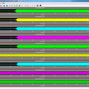
We present a novel generalization of quadrature oscillators (QVCO) which we call “arbitrary phase oscillator” or APO for short. In contrast to a QVCO which generates only quadrature phases, the APO is capable of continuously generating any desired phase at its output. The proposed structure employs a novel coupling mechanism to generate arbitrary phase shifts between two coupled oscillators without the need for an explicit phase shifter. A rigorous nonlinear dynamic analysis is presented to give a closed-form formula for the generated phase shifts, and the theory is verified by numerical simulation as well as measurement results of a prototype chip fabricated in 130-nm CMOS technology. The prototype APO has a frequency tuning range of 4.90–5.65 GHz and is continuously phase tunable from 0◦ to 360◦ across the entire frequency range. The APO structure can be used in designing novel coupled-oscillator-based phased arrays for 5G wireless communications.
List of the following materials will be included with the Downloaded Backup:A Two-Speed, Radix-4, Serial–Parallel Multiplier (Booth Multiplier )
Abstract:
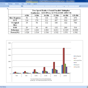
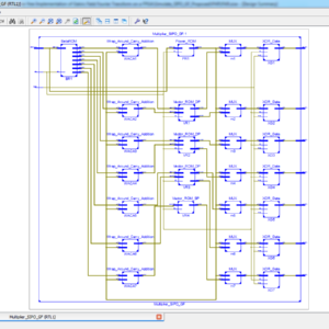
In this paper, we present a two-speed, radix-4, serial-parallel multiplier for accelerating applications such as digital filters, artificial neural networks, and other machine learning algorithms. Our multiplier is a variant of the serial–parallel (SP) modified radix-4 Booth multiplier that adds only the nonzero Booth encodings and skips over the zero operations, making the latency dependent on the multiplier value. Two sub circuits with different critical paths are utilized so that throughput and latency are improved for a subset of multiplier values. The multiplier is evaluated on an Intel Cyclone V field-programmable gate array against standard parallel–parallel and SP multipliers across four different process–voltage–temperature corners. We show that for bit widths of 32 and 64, our optimizations can result in a 1.42×–3.36× improvement over the standard parallel Booth multiplier in terms of area–time depending on the input set.
List of the following materials will be included with the Downloaded Backup:An Analog LO Harmonic Suppression Technique for SDR Receivers
Abstract:
A low-complexity analog technique to suppress the local oscillator (LO) harmonics in software-defined radios is presented. Accurate mathematical analyses show that an effective attenuation of the LO harmonics is achieved by modulating the transconductance of the low-noise transconductance amplifier (LNTA) with a raised-cosine signal. This modulation is performed through the bias network of a cascode device with a negligible increase in the LNTA noise figure. The proposed technique results in a notch at the third harmonic and at least 36 dB of attenuation at the fifth and the seventh harmonics. Experimental results in 130-nm CMOS and post layout simulation results in 65-nm CMOS verify the proper functionality of the proposed technique and the accuracy of the proposed analyses
List of the following materials will be included with the Downloaded Backup:Analysis, Comparison, and Experimental Validation of a Class AB Voltage Follower With Enhanced Bandwidth and Slew Rate
Abstract:
This paper describes a bandwidth (BW)- and slew rate (SR)-enhanced class AB voltage follower (VF). A thorough small signal analysis of the proposed and a state-of-the-art AB-enhanced VF is presented to compare their performance. The proposed circuit has 50-MHz BW, 19.5-V/µs SR, and a BW figure of merit of 41.6 (MHz × pF/µW) for CL = 50 pF. It provides 13 times higher current efficiency and 15 times higher BW than the conventional VF with equal 60-µW static power dissipation. The experimental and simulation results of a fabricated test chip in the 130-nm CMOS technology validate the proposed circuit.
List of the following materials will be included with the Downloaded Backup:Area-Efficient Bidirectional Shift-Register Using Bidirectional Pulsed-Latches
Abstract:
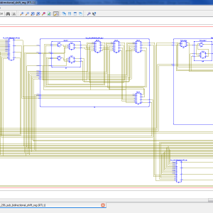
This paper proposes an area-efficient bidirectional shift-register using bidirectional pulsed-latches. The proposed bidirectional shift-register reduces the area and power consumption by replacing master-slave flip-flops and 2-to-1 multiplexers with the proposed bidirectional pulsed-latches and non-overlap delayed pulsed clock signals, and by using sub shift-registers and extra temporary storage latches. A 256-bit bidirectional shift-register was fabricated using a 65nm CMOS process. Its area was 1,943μm2 and its power consumption is 200μW at a 100MHz clock frequency with VDD=1.2V. It reduces area by 39.2% and power consumption by 19.4% compared to the conventional bidirectional shift-register, length in most cases.
List of the following materials will be included with the Downloaded Backup:Area-Time Efficient Streaming Architecture for FAST and BRIEF Detector
Abstract:
The combination of FAST corners and BRIEF descriptors provide highly robust image features. We present a novel detector for computing the FAST-BRIEF features from streaming images. To reduce the complexity of the BRIEF descriptor, we employ an optimized adder tree to perform summation by accumulation on streaming pixels for the smoothing operation. Since the window buffer used in existing designs for computing the BRIEF point-pairs are often poorly utilized, we propose an efficient sampling scheme that exploits register reuse to minimize the number of registers. Synthesis results based on 65- nm CMOS technology show that the proposed FAST-BRIEF core achieves over 40% reduction in area-delay product compared to the baseline design. In addition, we show that the proposed architecture can achieve 1.4x higher throughput than the baseline architecture with slightly lower energy consumption.
List of the following materials will be included with the Downloaded Backup:Chaos-Based Bitwise Dynamical Pseudorandom Number Generator on FPGA
Abstract:
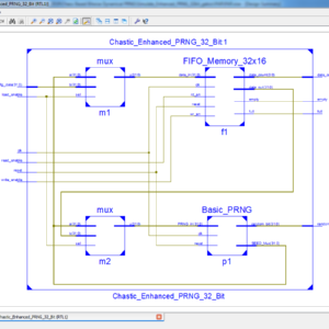
In this paper, a new pseudorandom number generator (PRNG) based on the logistic map has been proposed. To prevent the system to fall into short period orbits as well as increasing the randomness of the generated sequences, the proposed algorithm dynamically changes the parameters of the chaotic system. This PRNG has been implemented in a vertex 7 field-programmable gate array (FPGA) with a 32-bit fixed point precision, using a total of 510 lookup tables (LUTs) and 120 registers. The sequences generated by the proposed algorithm have been subjected to the National Institute of Standards and Technology (NIST) randomness tests, passing all of them. By comparing the randomness with the sequences generated by a raw 32-bit logistic map, it is shown that, by using only an additional 16% of LUTs, the proposed PRNG obtains a much better performance in terms of randomness, increasing the NIST passing rate from 0.252 to 0.989. Finally, the proposed bitwise dynamical PRNG is compared with other chaos-based realizations previously proposed, showing great improvement in terms of resources and randomness.
List of the following materials will be included with the Downloaded Backup:CMOS First-Order All-Pass Filter With 2-Hz Pole Frequency
Abstract:
A CMOS fully integrated all-pass filter with an extremely low pole frequency of 2 Hz is introduced in this paper. It has 0.08-dB passband ripple and 0.029-mm2Si area. It has 0.38-mW power consumption in strong inversion with ±0.6-V power supplies. In subthreshold, it has 0.64-µW quiescent power and operates with ±200-mV dc supplies. Miller multiplication is used to obtain a large equivalent capacitor without excessive Si area. By varying the gain of the Miller amplifier, the pole frequency can be varied from 2 to 48 Hz. Experimental and simulation results of a test chip prototype in 130-nm CMOS technology validate the proposed circuit.
List of the following materials will be included with the Downloaded Backup:Column-Selection-Enabled 10T SRAM Utilizing Shared Diff-VDD Write and Dropped-VDD Read for Power Reduction
Abstract:
A non-destructive column-selection-enabled 10T SRAM for aggressive power reduction is presented in this brief. It frees a half-selected behavior by exploiting the bit line-shared data-aware write scheme. The differential-VDD (Diff-VDD) technique is adopted to improve the write ability of the design. In addition, its decoupled read bit lines are given permission to be charged and discharged depending on the stored data bits. In combination with the proposed dropped-VDD biasing, it achieves the significant power reduction. The experimental results show that the proposed design provides the 3.3× improvement in the write margin compared with the standard Diff-10T SRAM. A 5.5-kb 10T SRAM in a 65-nm CMOS process has a total power of 51.25 µW and a leakage power of 41.8 µW when operating at 6.25 MHz at 0.5 V, achieving 56.3% reduction in dynamic power and 32.1% reduction in leakage power compared with the previous single-ended 10T SRAM.
List of the following materials will be included with the Downloaded Backup:Constant Time Hardware Architecture for a Gaussian Smoothing Filter
Abstract:
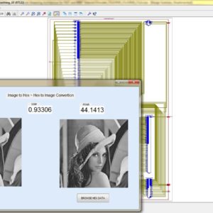
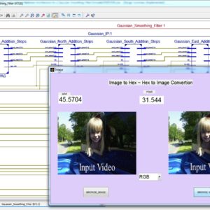
In this paper a new and highly efficient hardware architecture for a bit-serial implementation of a 3*3 filter on FPGA is developed and presented. The concept is implemented on a Gaussian blur spatial filter and it can be extended to other filters with similar characteristics. The proposed Single Instruction Multiple Data (SIMD) architecture provides a constant operating time independent of the size of the given image while the arithmetic operations are limited to the operations of addition. The Multiple Instruction Multiple Data (MIMD) performance is achieved in a near fraction of the cost. Thus, the hardware’s utilization is optimized. The total time needed to perform the filter of interest on the given image is solely dependent on the working clock frequency. The proposed design is evaluated using a small image and is implemented on two FPGA families with various sizes of an image. Also, it is compared with other architectures.
List of the following materials will be included with the Downloaded Backup:Design of Reconfigurable Digital IF Filter with Low Complexity
Abstract:
Due to limited frequency resources, new services are being applied to the existing frequencies, and service providers are allocating some of the existing frequencies for newly enhanced mobile communications. Because of this frequency environment, repeater and base station systems for mobile communications are becoming more complicated, and frequency interference caused by multiple bands and services is getting worse. Therefore, a heterodyne receiver using IF filters with high selectivity has been used to minimize the interference between frequencies. However, repeater and base station systems in mobile communications employing fixed IF filters cannot actively cope with the usage of multiple frequency bands, the application of various services, and frequency recycling. Therefore, this brief proposes a reconfigurable digital IF filter with variable center frequency and bandwidth while achieving high selectivity as existing IF filters. The center frequency of filter can vary from 10MHz to 62.5MHz, and the filter bandwidth can be selective to one of 10MHz, 15MHz, and 20MHz. The proposed digital filter also reduces the complexity of adders and multipliers by 38.81% and 41.57%, respectively, compared to an existing digital filter by using a filter bank and a multi stage structure. This digital IF filter is fabricated on a 130-nm CMOS process and occupies 5.90 mm2.
List of the following materials will be included with the Downloaded Backup:Design of Sparse FIR Filters With Reduced Effective Length
Abstract:
In this paper, an exchange algorithm is proposed to design sparse linear phase finite impulse response (FIR) filters with reduced effective length. The sparse FIR filter design problem is formally an l0-norm minimization problem. This original design problem is re-formulated by encoding the filter coefficients using a binary encoding vector, which represents the locations of the zero and non-zero filter coefficients. An iterative 0-1 exchange process with proper direction control is proposed to propel the minimax approximation error toward the specified upper bound of error for sparsity maximization. The effective length is optimized with a lower priority than sparsity in the proposed algorithm. Simulation results show that the proposed algorithm is superior to the existing algorithms in terms of both sparsity and/or effective length in most cases.
List of the following materials will be included with the Downloaded Backup:Efficient Design for Fixed-Width Adder-Tree
Abstract:
Conventionally, fixed-width adder-tree (AT) design is obtained from the full-width AT design by employing direct or post-truncation. In direct-truncation, one lower order bit of each adder output of full-width AT is post-truncated, and in case of post-truncation, {p} lower order-bits of final-stage adder output are truncated, where p = dlog2 Ne and N is the input-vector size. Both these methods do not provide an efficient design. In this paper, a novel scheme is presented to obtain fixed-width AT design using truncated input. A bias estimation formula based on probabilistic approach is presented to compensate the truncation error. The proposed fixed-width AT design for input-vector sizes 8 and 16 offers (37%, 23%, 22%) and (51%, 30%, 27%) area delay product (ADP) saving for word-length sizes (8, 12, 16), respectively, and calculates the output almost with the same accuracy as the post-truncated fixed-width AT which has the highest accuracy among the existing fixed-width AT. Further, we observed that Walsh-Hadamard transform based on the proposed fixed-width AT design reconstruct higher-texture images with higher peak signal to noise ratio (PSNR) and moderate-texture images with almost the same PSNR compared to those obtained using the existing AT designs. Besides, the proposed design creates an additional advantage to optimize other blocks appear at the upstream of the AT in a complex design.
List of the following materials will be included with the Downloaded Backup:Energy-Quality Scalable Adders Based on Non-zeroing Bit Truncation
Abstract:
Approximate addition is a technique to trade off energy consumption and output quality in error-tolerant applications. In prior art, bit truncation has been explored as a lever to dynamically trade off energy and quality. In this brief, an innovative bit truncation strategy is proposed to achieve more graceful quality degradation compared to state-of-the-art truncation schemes. This translates into energy reduction at a given quality target. When applied to a ripple-carry adder, the proposed bit truncation approach improves quality by up to 8.5 dB in terms of peak signal-to-noise ratio, compared to traditional bit truncation. As a case study, the proposed approach was applied to a discrete cosine transform engine. In comparison with prior art, the proposed approach reduces energy by 20%, at insignificant delay and silicon area overhead.
List of the following materials will be included with the Downloaded Backup:Error Detection and Correction in SRAM Emulated TCAMs
Abstract:
Ternary content addressable memories (TCAMs) are widely used in network devices to implement packet classification. They are used, for example, for packet forwarding, for security, and to implement software-defined networks (SDNs). TCAMs are commonly implemented as standalone devices or as an intellectual property block that is integrated on networking application-specific integrated circuits. On the other hand, field-programmable gate arrays (FPGAs) do not include TCAM blocks. However, the flexibility of FPGAs makes them attractive for SDN implementations, and most FPGA vendors provide development kits for SDN. Those need to support TCAM functionality and, therefore, there is a need to emulate TCAMs using the logic blocks available in the FPGA. In recent years, a number of schemes to emulate TCAMs on FPGAs have been proposed. Some of them take advantage of the large number of memory blocks available inside modern FPGAs to use them to implement TCAMs. A problem when using memories is that they can be affected by soft errors that corrupt the stored bits. The memories can be protected with a parity check to detect errors or with an error correction code to correct them, but this requires additional memory bits per word. In this brief, the protection of the memories used to emulate TCAMs is considered. In particular, it is shown that by exploiting the fact that only a subset of the possible memory contents are valid, most single-bit errors can be corrected when the memories are protected with a parity bit.
List of the following materials will be included with the Downloaded Backup:Feed forward-Cutset-Free Pipelined Multiply–Accumulate Unit for the Machine Learning Accelerator
Abstract:
Multiply–accumulate (MAC) computations account for a large part of machine learning accelerator operations. The pipelined structure is usually adopted to improve the performance by reducing the length of critical paths. An increase in the number of flip-flops due to pipelining, however, generally results in significant area and power increase. A large number of flip-flops are often required to meet the feed forward-cutset rule. Based on the observation that this rule can be relaxed in machine learning applications, we propose a pipelining method that eliminates some of the flip-flops selectively. The simulation results show that the proposed MAC unit achieved a 20% energy saving and a 20% area reduction compared with the conventional pipelined MAC.
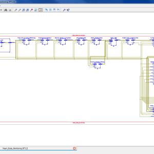
List of the following materials will be included with the Downloaded Backup:FPGA Heart Rate Monitoring (Pre Processing – QRS Detection Stage)
Base Paper Abstract:
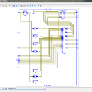
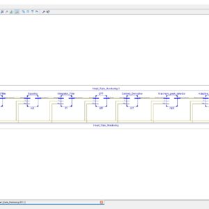
The continuous monitoring of cardiac patients requires an ambulatory system that can automatically detect heart diseases. This study presents a new field programmable gate array (FPGA)-based hardware implementation of the QRS complex detection. The proposed detection system is mainly based on the Pan and Tompkins algorithm, but applying a new, simple, and efficient technique in the detection stage. The new method is based on the centered derivative and the intermediate value theorem, to locate the QRS peaks. The proposed architecture has been implemented on FPGA using the Xilinx System Generator for digital signal processor and the Nexys-4 FPGA evaluation kit. To evaluate the effectiveness of the proposed system, a comparative study has been performed between the resulting performances and those obtained with existing QRS detection systems, in terms of reliability, execution time, and FPGA resources estimation. The proposed architecture has been validated using the 48 half-hours of records obtained from the Massachusetts Institute of Technology - Beth Israel Hospital (MITBIH) arrhythmia database. It has also been validated in real time via the analogue discovery device.
List of the following materials will be included with the Downloaded Backup:FPGA-Based System For Heart Rate Monitoring
Abstract:
The continuous monitoring of cardiac patients requires an ambulatory system that can automatically detect heart diseases. This study presents a new field programmable gate array (FPGA)-based hardware implementation of the QRS complex detection. The proposed detection system is mainly based on the Pan and Tompkins algorithm, but applying a new, simple, and efficient technique in the detection stage. The new method is based on the centred derivative and the intermediate value theorem, to locate the QRS peaks. The proposed architecture has been implemented on FPGA using the Xilinx System Generator for digital signal processor and the Nexys-4 FPGA evaluation kit. To evaluate the effectiveness of the proposed system, a comparative study has been performed between the resulting performances and those obtained with existing QRS detection systems, in terms of reliability, execution time, and FPGA resources estimation. The proposed architecture has been validated using the 48 half-hours of records obtained from the Massachusetts Institute of Technology - Beth Israel Hospital (MITBIH) arrhythmia database. It has also been validated in real time via the analogue discovery device.
List of the following materials will be included with the Downloaded Backup:Highly Linear Low-Power Wireless RF Receiver for WSN
Abstract:
This paper introduces a low-power wireless RF receiver for the wireless sensor network. The receiver has improved linearity with incorporated current-mode circuits and high-selectivity filtering. The receiver operates at the 900-MHz industrial, scientific, and medical band and is implemented in 130-nm CMOS technology. The receiver has a frequency multiplication mixer, which uses a 300-MHz clock from a local oscillator (LO). The LO is implemented using vertical delay cells to reduce power consumption. The receiver conversion gain is 40 dB and the receiver noise. The receiver’s input third-order intercept point (IIP3) is −6 dBm and the total power consumption is 1.16 mW.
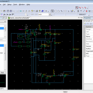
List of the following materials will be included with the Downloaded Backup:Instantaneous Power Consuming Level Shifter for Improving Power Conversion Efficiency of Buck Converter
Abstract:
An instantaneous power consuming level shifter is presented in this paper to increase the DC converter efficiency. The level shifter is used in a high-side power switch driver to remove the external capacitor which is used in bootstrap technique. The level shifter consumes power only during the transition period. A delay cell is used to turn the level shifter off to reduce the power consumption period. An output voltage detector is added to turn the level shifter off even before the delay time. An asynchronous discontinuous conduction mode buck converter is designed to verify the performance of the level shifter. Simulation results show that the power consumption of the proposed level shifter decreased by 66%, while the converter efficiency increased by the maximum of 9% compared to results obtained for a conventional level shifter. The converter is fabricated using the TSMC 0.18-µm BCD process and it operates within an input range of 2–5 V when the current varies from 400 µA to 18 mA and delivers an output voltage of 1.8 V.
List of the following materials will be included with the Downloaded Backup:Line Coding Techniques for Channel Equalization: Integrated Pulse-Width Modulation and Consecutive Digit Chopping
Abstract:
This paper presents two new line-coding schemes, integrated pulse width modulation (iPWM) and consecutive digit chopping (CDC) for equalizing lossy wire line channels with the aim of achieving energy efficient wire line communication. The proposed technology friendly encoding schemes are able to overcome the fundamental limitations imposed by Manchester or pulse-width modulation encoding on high-speed wire line transceivers. A highly digital encoder architecture is leveraged to implement the proposed iPWM and CDC encoding. Energy-efficient operation of the proposed encoding is demonstrated on a high-speed wire line transceiver that can operate from 10 to 18 Gb/s. Fabricated in a 65-nm CMOS process, the transceiver operates with supply voltages of 0.9 V, 1 V, and 1.1 V. With the help of the proposed iPWM encoding, the transceiver can equalize over 27-dB of channel loss while operating at 16 Gb/s with an efficiency of 4.37 pJ/bit. The design occupies an active die area of 0.21 mm2.
List of the following materials will be included with the Downloaded Backup:Low-Complexity 2-D Digital FIR Filters Using Polyphase Decomposition and Farrow Structure
Abstract:
This paper proposes a novel realization technique for quadrantally symmetric 2-D finite impulse response filters with a guaranteed reduction in the hardware complexity. Here, the concept of Farrow structure-based interpolation filter design using the polyphase decomposition of the 1-D filter transfer function is effectively utilized in the 2-D domain. The proposed 2-D filter makes use of row-wise polyphase decomposition of the 2-D transfer function or frequency response, followed by the polynomial approximation of the individual polyphase coefficients resulting in Farrow structures corresponding to each row filter. The final coefficients are implemented by varying the delay values in all the Farrow structures, followed by the interpolation of the coefficients obtained from each delay value, which in turn forms the rows in the 2-D kernel. The major highlight of the proposed method is the highly reduced implementation complexity in terms of the number of multipliers and adders, with a low normalized root-mean-square error. Design examples of the circularly symmetric and fan-type filters have been considered to show the efficiency of the approach. The results show a drastic reduction in the implementation complexity of the 2-D filters of upto 20%, with significantly low normalized root-mean-square error lesser than 0.5%.
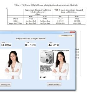
List of the following materials will be included with the Downloaded Backup:Low-Power Approximate Unsigned Multipliers with Configurable Error Recovery
Abstract:
Approximate circuits have been considered for applications that can tolerate some loss of accuracy with improved performance and/or energy efficiency. Multipliers are key arithmetic circuits in many of these applications including digital signal processing (DSP). In this paper, a novel approximate multiplier with a low power consumption and a short critical path is proposed for high-performance DSP applications. This multiplier leverages a newly designed approximate adder that limits its carry propagation to the nearest neighbors for fast partial product accumulation. Different levels of accuracy can be achieved by using either OR gates or the proposed approximate adder in a configurable error recovery. The multipliers using these two error reduction strategies are referred to as approximate multiplier 1 (AM1) and approximate multiplier 2 (AM2), respectively. Both AM1 and AM2 have a low mean error distance, i.e., most of the errors are not significant in magnitude. Compared to a Wallace multiplier optimized for speed, an 8×8 AM1 with 4 MSBs (most significant bits) for error reduction and synthesized using a 28 nm CMOS process shows a 60% reduction in delay (when optimized for delay) and a 42% reduction in power dissipation (when optimized for area). In a 16×16 design, half of the least significant partial products are truncated for AM1 and AM2, which are thus denoted as TAM1 and TAM2, respectively. Compared with the Wallace multiplier, TAM1 and TAM2 save from 50% to 66% in power, when optimized for area. Compared to existing approximate multipliers, AM1, AM2, TAM1 and TAM2 show significant advantages in accuracy with a high performance. AM2 has a better accuracy compared to AM1 but with a longer delay and higher power consumption. Image processing applications including image sharpening and smoothing are considered to show the quality of the approximate multipliers in error-tolerant applications. By utilizing an appropriate error recovery, the proposed approximate multipliers achieve similar processing accuracy as traditional exact multipliers, but with significant improvements in power.
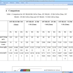
List of the following materials will be included with the Downloaded Backup:Low-Power Near-Threshold 10T SRAM Bit Cells With Enhanced Data-Independent Read Port Leakage for Array Augmentation in 32-nm CMOS
Abstract:
The conventional six-transistor static random access memory (SRAM) cell allows high density and fast differential sensing but suffers from half-select and read-disturb issues. Although the conventional eight-transistor SRAM cell solves the read-disturb issue, it still suffers from low array efficiency due to deterioration of read bit-line (RBL) swing and Ion/Ioff ratio with increase in the number of cells per column. Previous approaches to solve these issues have been afflicted by low performance, data dependent leakage, large area, and high energy per access. Therefore, in this paper, we present three iterations of SRAM bit cells with nMOS-only based read ports aimed to greatly reduce data dependent read port leakage to enable 1k cells/RBL, improve read performance, and reduce area and power over conventional and 10T cell-based works. We compare the proposed work with other works by recording metrics from the simulation of a 128-kb SRAM constructed with divided-word line-decoding architecture and a 32-bit word size. Apart from large improvements observed over conventional cells, up to 100-mV improvement in read-access performance, up to 19.8% saving in energy per access, and up to 19.5% saving in the area are also observed over other 10T cells, thereby enlarging the design and application gamut for memory designers in low-power sensors and battery-enabled devices.
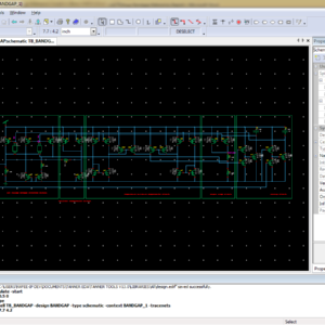
List of the following materials will be included with the Downloaded Backup:Low-Voltage Bandgap Reference Circuit in 28nm CMOS
Abstract:
This paper presents a hybrid adjusted temperature compensation circuit for reducing the temperature drift of the bandgap reference. Combining first-order bandgap current, nonlinear compensation current, and temperature curvature compensation current together, a temperature insensitive reference voltage can be obtained in proposed circuit. Designed and verified in UMC 28nm CMOS technology with Cadence IC615, the proposed circuit achieves a post-layout simulation temperature drift of 5.48 ppm/°C in the range of -20°C to 120°C with a supply voltage of 1.05-V.
List of the following materials will be included with the Downloaded Backup:Many-Objective Sizing Optimization of a Class-C/D VCO for Ultralow-Power IoT and Ultralow Phase-Noise Cellular Applications
Abstract:
In this paper, the performance boundaries and corresponding tradeoffs of a complex dual-mode class-C/D voltage controlled oscillator (VCO) are extended using a framework for the automatic sizing of radio frequency integrated circuit blocks, where an all-inclusive test bench formulation enhanced with an additional measurement processing system enables the optimization of “everything at once” toward its true optimal tradeoffs. VCOs embedded in the state-of-the-art multi standard transceivers must comply with extremely high performance and ultralow power requirements for modern cellular and Internet of Things applications. However, the proper analysis of the design tradeoffs is tedious and impractical, as a large amount of conflicting performance figures obtained from multiple modes, test benches, and/or analysis must be considered simultaneously. Here, the dual-mode design and optimization conducted provided 287 design solutions with figures of merit above 192 dBc/Hz, where the power consumption varies from 0.134 to 1.333 mW, the phase noise at 10 MHz from −133.89 to −142.51 dBc/Hz, and the frequency pushing from 2 to 500 MHz/V, on the worst case of the tuning range. These results pushed this circuit design to its performance limits on a 65-nm CMOS technology, reducing 49% of the power consumption of the original design while also showing its potential for ultralow power with more than 93% reduction. In addition, worst case corner criteria were also performed on the top of the worst case tuning range optimization, taking the problem to a human-untrea table LXVI-D performance space.
List of the following materials will be included with the Downloaded Backup:Multiloop Control for Fast Transient DC–DC Converter
Abstract:
A novel ac coupled feedback (ACCF) is proposed to alternatively realize fast transient response while inherently controlling the start-up in-rush current of a dc–dc switching converter. The proposed ACCF is modified from a conventional capacitor multiplier and connected between the outputs of the converter and the transconductance. With this supplemental feedback, the transient response has been significantly improved due to the gain-boosting effect around the compensator’s midband. Moreover, the ACCF circuit assists to manage the ramping speed of the output voltage during power-up, thereby eliminating the bulky soft-start circuit. The new controller is very simple to implement and occupies a tiny footprint on-chip. A buck converter with the proposed scheme has been fabricated using the 0.18-µm standard CMOS process with an active silicon area of 0.573 mm2. Measurement results show that the output voltage rises linearly for a soft-start period of 1.05 ms according to the designed slope. Excellent load transient responses are achieved under different load current steps; the output voltage overshoot/undershoot of 60 mV settles down within 10 µs for a load variation from 50 µA to 1 A in 1 µs. Moreover, the proposed converter maintains both excellent load and line regulations of 0.018 mV/mA and 0.0056 mV/mV, respectively.
List of the following materials will be included with the Downloaded Backup:Multiplier-free Implementation of Galois Field Fourier Transform on a FPGA
Abstract:
A novel approach to implementing Galois Field Fourier Transform (GFT) is proposed that completely eliminates the need for any finite field multipliers by transforming the symbols from a vector representation to a power representation. The proposed method is suitable for implementing GFTs of prime and nonprime lengths on modern FPGAs that have a large amount of on-chip distributed embedded memory. For GFT of length 255 that is widely used in many applications, the proposed memory based implementation exhibits 25% improvement in latency, 27% improvement in throughput, and 56% reduction in power consumption compared to a finite field multiplier based implementation.
List of the following materials will be included with the Downloaded Backup:New Majority Gate Based Parallel BCD Adder Designs for Quantum-dot Cellular Automata
Abstract:
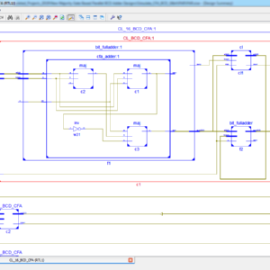
In this paper, we first theoretically re-defined output decimal carry in terms of majority gates and proposed a carry look ahead structure for calculating all the intermediate output carries. We have used this method for designing the multi-digit decimal adders. Theoretically, our best n-digit decimal adder design reduces the delay and area-delay product (ADP) by 50% compared with previous designs. We have implemented our designs using QCA Designer tool. The proposed QCA Designer based 8-digit PBA-BCD adder achieves over 38% less delay compared with the best existing designs.
List of the following materials will be included with the Downloaded Backup:Radiation-Hardened 14T SRAM Bit cell With Speed and Power Optimized for Space Application
Abstract:
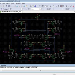
In this paper, a novel radiation-hardened 14-transistor SRAM bit cell with speed and power optimized [radiation-hardened with speed and power optimized (RSP)-14T] for space application is proposed. By circuit- and layout-level optimization design in a 65-nm CMOS technology, the 3-D TCAD mixed-mode simulation results show that the novel structure is provided with increased resilience to single-event upset as well as single-event–multiple-node upsets due to the charge sharing among OFF-transistors. Moreover, the HSPICE simulation results show that the write speed and power consumption of the proposed RSP-14T are improved by ∼65% and ∼50%, respectively, compared with those of the radiation hardened design (RHD)-12T memory cell.
List of the following materials will be included with the Downloaded Backup:Static Delay Variations Modules For Ripple-Carry and Borrow Save Adders
Abstract:
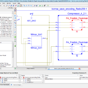
This paper introduces two statistical delay variability models for certain hardware adder implementations, namely, the ripple-carry adder (RCA) and the borrow-save adder (BSA). The introduced models take into account correlated variation sources. Initially, we derive a first proposed model, namely, Type-I model, in the form of expressions for the computation of the exact Probability Density Functions (PDFS) of maximum output delays for Gaussian and non-Gaussian variation sources. Furthermore, we present closed formulas for the co-variances between output delays of the aforementioned adder architectures. The introduced derived co-variances are subsequently combined with Clark’s method to derive a second proposed model, Type-II model, which comprises approximations of the maximum delay PDF for an RCA and a BSA. Simulation results and the derived exact Type-I PDFs are found to perfectly agree, while the proposed Clark-based Type-II models present an error for standard deviation of maximum delay that increases as BSA word length increases. Both the introduced models and the simulations prove that BSAs achieve narrower delay distributions than RCAs, i.e., they significantly reduce delay variance. Consequently, BSAs are proven to be suitable for variation-tolerant applications by providing a timing safety margin, when compared to RCA architectures. The underlying analysis indicates that for the case of BSA and either intra-die delay variations only or both intra and inter-die delay variations, the Type-II models introduce non negligible errors, which are as much as 16% of the standard deviation of maximum delay for a 256-digit BSA, as the Type II Gaussian PDF approximations deviate significantly from the exact Type-I PDFs. However, for all RCA and BSA inter-die only variation cases, both types present satisfactory accuracy due to the Gaussian shape of exact PDF.
List of the following materials will be included with the Downloaded Backup:TOSAM: An Energy-Efficient Truncation- and Rounding-Based Scalable Approximate Multiplier
Abstract:
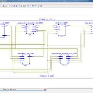
A scalable approximate multiplier, called truncation- and rounding-based scalable approximate multiplier (TOSAM) is presented, which reduces the number of partial products by truncating each of the input operands based on their leading one-bit position. In the proposed design, multiplication is performed by shift, add, and small fixed-width multiplication operations resulting in large improvements in the energy consumption and area occupation compared to those of the exact multiplier. To improve the total accuracy, input operands of the multiplication part are rounded to the nearest odd number. Because input operands are truncated based on their leading one-bit positions, the accuracy becomes weakly dependent on the width of the input operands and the multiplier becomes scalable. Higher improvements in design parameters (e.g., area and energy consumption) can be achieved as the input operand widths increase. To evaluate the efficiency of the proposed approximate multiplier, its design parameters are compared with those of an exact multiplier and some other recently proposed approximate multipliers. Results reveal that the proposed approximate multiplier with a mean absolute relative error in the range of 11%–0.3% improves delay, area, and energy consumption up to 41%, 90%, and 98%, respectively, compared to those of the exact multiplier. It also outperforms other approximate multipliers in terms of speed, area, and energy consumption. The proposed approximate multiplier has an almost Gaussian error distribution with a near-zero mean value. We exploit it in the structure of a JPEG encoder, sharpening, and classification applications. The results indicate that the quality degradation of the output is negligible. In addition, we suggest an accuracy configurable TOSAM where the energy consumption of the multiplication operation can be adjusted based on the minimum required accuracy.
List of the following materials will be included with the Downloaded Backup:World’s Fastest FFT Architectures: Breaking the Barrier of 100 GS/s
Abstract:
This paper presents the fastest fast Fourier transform (FFT) hardware architectures so far. The architectures are based on a fully parallel implementation of the FFT algorithm. In order to obtain the highest throughput while keeping the resource utilization low, we base our design on making use of advanced shift-and-add techniques to implement the rotators and on selecting the most suitable FFT algorithms for these architectures. Apart from high throughput and resource efficiency, we also guarantee high accuracy in the proposed architectures. For the implementation, we have developed an automatic tool that generates the architectures as a function of the FFT size, input word length and accuracy of the rotations. We provide experimental results covering various FFT sizes, FFT algorithms, and field-programmable gate array boards. These results show that it is possible to break the barrier of 100 GS/s for FFT calculation.
List of the following materials will be included with the Downloaded Backup:IEEE Transactions on VLSI, VLSI IEEE Project, VLSI Low Power Project, VLSI High Speed Project, VLSI Area Efficient Project, Low Cost VLSI Projects, High Speed VLSI Design projects ( CDMA, RTOS, DSP, RF, IF, etc), Low Power VLSI Design projects, Area Efficient VLSI Design projects , Audio processing VLSI Design projects, Signal Processing VLSI Design projects, Image Processing VLSI Design projects, Backend VLSI Design projects ( CMOS, TFET, BisFET, FeFET, etc), Timing & Delay Reduction VLSI Projects, Internet of Things VLSI Projects, Testing, Reliability and Fault Tolerance VLSI Projects, VLSI Applications ( Communicational, Video, Security, Sensor Networks, etc), SOC VLSI Projects, Network on Chip VLSI Projects, Wireless Communication VLSI Projects, VLSI Verifications Projects ( UVM, OVM, VVM, System Verilog.
Provide Wordlwide Online Support
We can provide Online Support Wordlwide, with proper execution, explanation and additionally provide explanation video file for execution and explanations.
24/7 Support Center
NXFEE, will Provide on 24x7 Online Support, You can call or text at +91 9789443203, or email us nxfee.innovation@gmail.com
Terms & Conditions:
Customer are advice to watch the project video file output, and before the payment to test the requirement, correction will be applicable.
After payment, if any correction in the Project is accepted, but requirement changes is applicable with updated charges based upon the requirement.
After payment the student having doubts, correction, software error, hardware errors, coding doubts are accepted.
Online support will not be given more than 3 times.
On first time explanation we can provide completely with video file support, other 2 we can provide doubt clarifications only.
If any Issue on Software license / System Error we can support and rectify that within end of day.
Extra Charges For duplicate bill copy. Bill must be paid in full, No part payment will be accepted.
After payment, to must send the payment receipt to our email id.
Powered by NXFEE INNOVATION, Pondicherry.
Call us today at : +91 9789443203 or Email us at nxfee.innovation@gmail.com
NXFEE Development & Services

Product Categories
- 2014 (11)
- 2015 (39)
- 2016 (30)
- 2017 (16)
- 2018 (17)
- 2019 (42)
- 2020 (29)
- 2021 (17)
- 2022 (23)
- Accessories (45)
- Area Efficient (117)
- High speed VLSI Design (57)
- IEEE (15)
- Image Processing (40)
- Low power VLSI Design (98)
- NOC VLSI Design (2)
- VLSI (251)
- VLSI 2023 (21)
- VLSI 2024 (18)
- VLSI 2025 (32)
- VLSI 2026 (4)
- VLSI Application / Interface and Mini Projects (31)
- VLSI_2023 (15)
Filter by price
Product Status
Sort by producents

Copyright © 2026 Nxfee Innovation.

