IEEE Transactions on VLSI 2018
Following Novelty based Research Projects not yet Published in Any Journal
Customization Available for Journal Publications
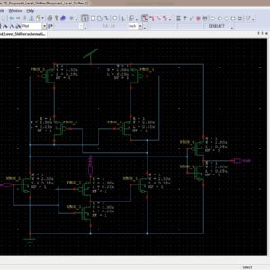
A Low Power and High Speed Voltage Level Shifter Based on a Regulated Cross Coupled Pull Up Network
Abstract:
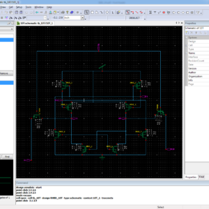
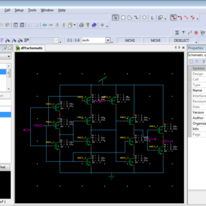
In this brief, a fast and very low power voltage level shifter (LS) is presented. By using a new regulated cross-coupled (RCC) pull-up network, the switching speed is boosted and the dynamic power consumption is highly reduced. The proposed (LS) has the ability to convert input signals with voltage levels much lower than the threshold voltage of a MOS device to higher nominal supply voltage levels. The presented LS occupies a small silicon area owing to its very low number of elements and is ultra-low-power, making it suitable for low-power applications such as implantable medical devices and wireless sensor networks. Results of the post-layout simulation in a standard 0.18-μm CMOS technology show that the proposed circuit can convert up input voltage levels as low as 80 mV. The power dissipation and propagation delay of the proposed level shifter for a low/high supply voltages of 0.4/1.8 V and input frequency of 1 MHz are 123.1 nW and 23.7 ns, respectively.
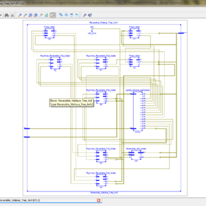
List of the following materials will be included with the Downloaded Backup:An Efficient Design for Reversible Wallace Unsigned Multiplier
Abstract:
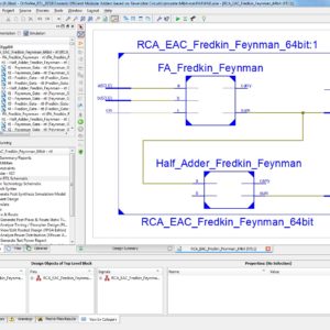
Today, reversible logic can be used for designing low-power CMOS circuits, optical data processing, DNA computations, biological researches, quantum circuits and nanotechnology. Sometimes using of reversible logic is inevitable such as build quantum computers. Reversible logic circuits structure is much more complicated than irreversible logic circuits. Multiplication operation is considered as one of the most important operations in the ALU unit. In this paper, we have proposed two 4×4 reversible unsigned multiplier circuits in which Wallace tree method is used to reduce the depth of circuits. In first design, the partial products circuit is designed using TG and FG gates so that TG is used to produce the partial products and FG for fan-out. In the second design, TG and PG gates are used to produce the partial products and no fan-out is required. Moreover, we have used PG gate and Feynman' block as reversible half-adder (HA) and full-adder (FA) in the summation network, respectively. In the first design, the main purpose is to decrease the depth of the circuit and increase the circuit speed. In the second design we would attempt to improve quantum parameters the number of garbage outputs, constant inputs and quantum cost. The evaluation results show that the first design, in terms of delay, is the fastest circuit. Also, the second design in terms of the number of constant inputs, garbage outputs and quantum cost is better than other designs.
List of the following materials will be included with the Downloaded Backup:An Efficient VLSI Architecture for Convolution Based DWT Using MAC
Abstract:
The modern real time applications related to image processing and etc., demand high performance discrete wavelet transform (DWT). This paper proposes the floating point multiply accumulate circuit (MAC) based 1D/2D-DWT, where the MAC is used to find the outputs of high/low pass FIR filters. The proposed technique is implemented with 45 nm CMOS technology and the results are compared with various existing techniques. The proposed 8 × 8-point floating point 2-levels 2D-DWT achieves 27.6% and 83.7% of reduction in total area and net power respectively as compared with existing DWT.
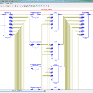
List of the following materials will be included with the Downloaded Backup:Approximate Sum-of-Products Design Based on Distributed Arithmetic
Proposed Abstract:
Approximate circuits provide high performance and require low power. Sum-of-products (SOP) units are key elements in many digital signal processing applications. In this brief, three approximate SOP (ASOP) models which are based on the distributed arithmetic are proposed. They are designed for different levels of accuracy. First model of ASOP achieves an improvement up to 64% on area and 70% on power, when compared with conventional unit. Other two models provide an improvement of 32% and 48% on area and 54% and 58% on power, respectively, with a reduced error rate compared with the first model. Third model achieves the mean relative error and normalized error distance as low as 0.05% and 0.009%, respectively. Performance of approximate units is evaluated with a noisy image smoothing application, where the proposed models are capable of achieving higher peak signal to-noise ratio than the existing state-of-the-art techniques. It is shown that the proposed approximate models achieve higher processing accuracy than existing works but with significant improvements in power and performance.
List of the following materials will be included with the Downloaded Backup:Combating Data Leakage Trojans in Commercial and ASIC Applications With Time-Division Multiplexing and Random Encoding
Proposed Abstract:
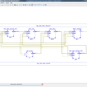
This paper explains the concept of reduction of data leakage Trajons in modulation scheme of TDM (Time Division Multiplexing) using DES (Data Encryption Standard) encoding and decoding concept. The DES is a symmetric key block cipher which is used for encryption and decryption process. In hardware manufacturing, detection and prevention of hardware Trajons attacks becomes a major concern for a manufacturing company. Because, the hardware Trajons is able to steal some sensitive information of a users such as encryption keys, passwords, etc,. So, most defensive methods prefers on prevention of data. The existing system uses the concept of RECORD ( Randomized encoding of combinational logic for resistance to data leakage) to prevent the data from the hardware Trajons even the Trajons known the entire information. Thus the proposed system of TDM version of RECORD design is more secure than the Sequential RECORD system and these case of existing work, will not concentrate and proved TDM RECORD DES Decryption Algorithm. Therefore, the proposed work of this paper will used the concept of TDM version using RECORD with implement in Encryption and Decryption Algorithm and also BER Testing, this method will have designed in Verilog HDL and implement in Xilinx FPGA and finally shown the comparison results in terms of area, delay and power.
List of the following materials will be included with the Downloaded Backup:Design and Implementation of Efficient Streaming Deblocking and SAO Filter for HEVC Decoder
We have also Code for 720 x 576 Image Resolution using 64 x 64 Block Size of HEVC. Cost of this Update work in High Resolution Rs. 45,000/- ( Rs. 45,000/- + Rs. 35,000/- ) : Total Cost : Rs. 80,000/-
Abstract:
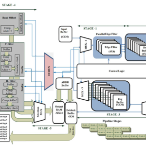
This paper aims to design an efficient mixed serial five-stage pipeline processing hardware architecture of deblocking filter (DBF) and sample adaptive offset (SAO) filter for high efficiency video coding decoder. The proposed hardware is designed to increase the throughput and reduce the number of clock cycles by processing the pixels in a stream of 4 × 36 samples in which edge filters are applied vertically in a parallel fashion for processing of luma/chroma samples. Subsequently these filtered pixels are transposed and reprocessed through vertical filter for horizontal filtering in a pipeline fashion. Finally, the filtered block transposed back to the original orientation and forwarded to a three-stage pipeline SAO filter. The proposed architecture is implemented in field programmable gate array and application specific integrated circuit platform using 90-nm library. Experimental results illustrate that the proposed DBF and SAO architecture decreases the processing cycles (172) required for processing each 64 × 64 or large coding unit compared with the state-of-the-art literature with the increase of gate count (593.32K) including memory. The results show that the throughput of the proposed filter can successfully decode ultrahigh definition video sequences at 200 frames/s at 341 MHz.
List of the following materials will be included with the Downloaded Backup:Design of Area-Efficient and Highly Reliable RHBD 10T Memory Cell for Aerospace Applications
Abstract:
In this brief, based on upset physical mechanism together with reasonable transistor size, a robust 10T memory cell is first proposed to enhance the reliability level in aerospace radiation environment, while keeping the main advantages of small area, low power, and high stability. Using Taiwan Semiconductor Manufacturing Company 65-nmCMOS commercial standard process, simulations performed in Cadence Spectre demonstrate the ability of the proposed radiation-hardened-by-design 10T cell to tolerate both 0 →1and1→0 single node upsets, with the increased read/write access time.
List of the following materials will be included with the Downloaded Backup:Efficient TCAM Design Based on Multipumping Enabled Multiported SRAM on FPGA
Abstract:
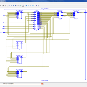
Ternary content-addressable memory (TCAM)-based search engines play an important role in networking routers. The search space demands of TCAM applications are constantly rising. However, existing realizations of TCAM on field-programmable gate arrays (FPGAs) suffer from storage inefficiency. This paper presents a multipumping-enabled multiported SRAM-based TCAM design on FPGA, to achieve an efficient utilization of SRAM memory. Existing SRAM-based solutions for TCAM reduce the impact of the increase in the traditional TCAM pattern width from an exponential growth in memory usage to a linear one using cascaded block RAMs (BRAMs) on FPGA. However, BRAMs on state-of-the-art FPGAs have a minimum depth limitation, which limits the storage efficiency for TCAM bits. Our proposed solution avoids this limitation by mapping the traditional TCAM table divisions to shallow sub-blocks of the configured BRAMs, thus achieving a memory-efficient TCAM memory design. The proposed solution operates the configured simple dual-port BRAMs of the design as multiported SRAM using the multipumping technique, by clocking them with a higher internal clock frequency to access the sub-blocks of the BRAM in one system cycle. We implemented our proposed design on a Virtex-6 xc6vlx760 FPGA device. Compared with existing FPGA-based TCAM designs, our proposed method achieves up to 2.85 times better performance per memory.
List of the following materials will be included with the Downloaded Backup:FIR Filter Design based on FPGA
Abstract:
FIR (Finite Impulse Response) Filters: the finite impulse response filter is the most basic components in digital signal processing systems are widely used in communications, image processing, and pattern recognition. Based on FPGA(editable logic device) to achieve FIR filter, not only take into account the fixed -function DSP-specific chip real-time, but also has the DSP processor flexibility. The combination of FPGA and DSP technology can further improve integration, increase work speed and expand system capabilities.
List of the following materials will be included with the Downloaded Backup:Gate diffusion input based 4-bit Vedic multiplier design
Abstract:
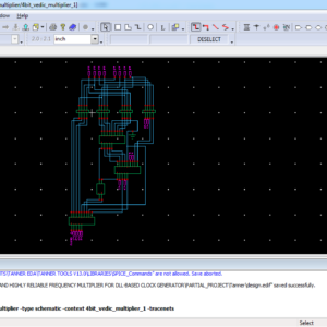
A multiplier is one of the key hardware blocks in most of the processors. Multiplication is a lengthy, time-consuming task. Vedic multiplication in field programmable gate array implementation has been proven effective in reducing the number of steps and circuit delay. Conventionally at the circuit level, complementary metal oxide semiconductor (CMOS) logic is used to design a multiplier. In CMOS circuits, the area is always an issue. Gate diffusion input (GDI)-based logic has been explored in the literature to reduce the number of transistors for various logic functions. Thus, Vedic mathematics, on the one hand, simplifies the multiplication process and reduces the delay; while on the other hand, GDI technique helps in minimizing the transistor count (TC) and reduction in power. Therefore, this study puts forth a GDI logic-based 4-bit Vedic multiplier. To study the effectiveness of the GDI logic, the transient response of a 2-bit Vedic multiplier using CMOS and GDI is compared. For the 4-bit Vedic multiplier, two design approaches are taken into consideration. The performance of these circuits is analyzed in terms of average power dissipation, delay, and TC. The effect of supply voltage scaling is also studied. The circuit simulations are carried out at 130 nm for bulk metal oxide semiconductor field effect transistor predictive technology model-based device parameters.
List of the following materials will be included with the Downloaded Backup:High speed and low power preset-able modified TSPC D flip-flop design and performance comparison with TSPC D flip-flop
Abstract:
Positron emission tomography (PET) is a nuclear functional imaging technique that produces a three-dimensional image of functional organs in the body. PET requires high resolution, fast and low power multichannel analog to digital converter (ADC). A typical multichannel ADC for PET scanner architecture consists of several blocks. Most of the blocks can be designed by using fast, low power D flip-flops. A preset-able true single phase clocked (TSPC) D flip-flop shows numerous glitches (noise) at the output due to unnecessary toggling at the intermediate nodes. Preset-able modified TSPC (MTSPC) D flip flop have been proposed as an alternative solution to alleviate this problem. However, the MTSPC D flip-flop requires one extra PMOS to suspend toggling of the intermediate nodes. In this work, we designed a 7-bit preset-able gray code counter by using the proposed D flip-flop. This work involves UMC 180 nm CMOS technology for preset-able 7-bit gray code counter where we achieved 1 GHz maximum operation frequency with most significant bit (MSB) delay 0.96 ns, power consumption 244.2 μW (micro watt) and power delay product (PDP) 0.23 pJ (Pico joule) from 1.8 V power supply.
List of the following materials will be included with the Downloaded Backup:Improving Error Correction Codes for Multiple-Cell Upsets in Space Applications
Proposed Abstract:
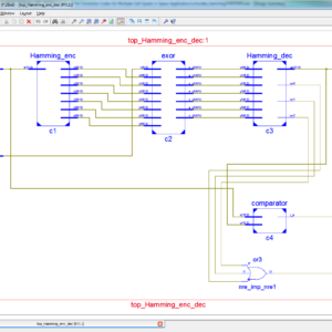
Currently, faults suffered by SRAM memory systems have increased due to the aggressive CMOS integration density. Thus, the probability of occurrence of single-cell upsets (SCUs) or multiple-cell upsets (MCUs) augments. One of the main causes of MCUs in space applications is cosmic radiation. A common solution is the use of error correction codes (ECCs). Nevertheless, when using ECCs in space applications, they must achieve a good balance between error coverage and redundancy, and their encoding/decoding circuits must be efficient in terms of area, power, and delay. Different codes have been proposed to tolerate MCUs. For instance, Matrix codes use Hamming codes and parity checks in a bi-dimensional layout to correct and detect some patterns of MCUs. Recently presented, column–line–code (CLC) has been designed to tolerate MCUs in space applications. CLC is a modified Matrix code, based on extended Hamming codes and parity checks. Nevertheless, a common property of these codes is the high redundancy introduced. In this paper, we present a series of new low redundant ECCs able to correct MCUs with reduced area, power, and delay overheads. Also, these new codes maintain, or even improve, memory error coverage with respect to Matrix and CLC codes.
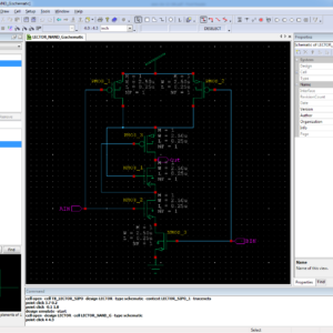
List of the following materials will be included with the Downloaded Backup:LECTOR: A Technique for Leakage Reduction in CMOS Circuits
Abstract:
In CMOS circuits, the reduction of the threshold voltage due to voltage scaling leads to increase in sub threshold leakage current and hence static power dissipation. We propose a novel technique called LECTOR for designing CMOS gates which significantly cuts down the leakage current without increasing the dynamic power dissipation. In the proposed technique, we introduce two leakage control transistors (a p-type and a n-type) within the logic gate for which the gate terminal of each leakage control transistor (LCT) is controlled by the source of the other. In this arrangement, one of the LCTs is always “near its cutoff voltage” for any input combination. This increases the resistance of the path from to ground, leading to significant decrease in leakage currents. The gate-level net list of the given circuit is first converted into a static CMOS complex gate implementation and then LCTs are introduced to obtain a leakage-controlled circuit. The significant feature of LECTOR is that it works effectively in both active and idle states of the circuit, resulting in better leakage reduction compared to other techniques. Further, the proposed technique overcomes the limitations posed by other existing methods for leakage reduction. Experimental results indicate an average leakage reduction of 79.4% for MCNC’91 benchmark circuits.
List of the following materials will be included with the Downloaded Backup:Low-Complexity VLSI Design of Large Integer Multipliers for Fully Homomorphic Encryption
Abstract:
Large integer multiplication has been widely used in fully homomorphic encryption (FHE). Implementing feasible large integer multiplication hardware is thus critical for accelerating the FHE evaluation process. In this paper, a novel and efficient operand reduction scheme is proposed to reduce the area requirement of radix-r butterfly units. We also extend the single port, merged-bank memory structure to the design of number theoretic transform (NTT) and inverse NTT (INTT) for further area minimization. In addition, an efficient memory addressing scheme is developed to support both NTT/INTT and resolving carries computations. Experimental results reveal that significant area reductions can be achieved for the targeted 786 432- and 1 179 648-bit NTT-based multipliers designed using the proposed schemes in comparison with the related works. Moreover, the two multiplications can be accomplished in 0.196 and 2.21 ms, respectively, based on 90-nm CMOS technology. The low-complexity feature of the proposed large integer multiplier designs is thus obtained without sacrificing the time performance.
List of the following materials will be included with the Downloaded Backup:Low-Power and Fast Full Adder by Exploring New XOR and XNOR Gates
Abstract:
In this paper, novel circuits for XOR/XNOR and simultaneous XOR–XNOR functions are proposed. The proposed circuits are highly optimized in terms of the power consumption and delay, which are due to low output capacitance and low short-circuit power dissipation. We also propose six new hybrid 1-bit full-adder (FA) circuits based on the novel full-swing XOR–XNOR or XOR/XNOR gates. Each of the proposed circuits has its own merits in terms of speed, power consumption, power delay product (PDP), driving ability, and so on. To investigate the performance of the proposed designs, extensive HSPICE and Cadence Virtuoso simulations are performed. The simulation results, based on the 65-nm CMOS process technology model, indicate that the proposed designs have superior speed and power against other FA designs. A new transistor sizing method is presented to optimize the PDP of the circuits. In the proposed method, the numerical computation particle swarm optimization algorithm is used to achieve the desired value for optimum PDP with fewer iterations. The proposed circuits are investigated in terms of variations of the supply and threshold voltages, output capacitance, input noise immunity, and the size of transistors.
List of the following materials will be included with the Downloaded Backup:Towards Efficient Modular Adders based on Reversible Circuits
Abstract:
Reversible logic is a computing paradigm that has attracted significant attention in recent years due to its properties that lead to ultra-low power and reliable circuits. Reversible circuits are fundamental, for example, for quantum computing. Since addition is a fundamental operation, designing efficient adders is a cornerstone in the research of reversible circuits. Residue Number Systems (RNS) has been as a powerful tool to provide parallel and fault-tolerant implementations of computations where additions and multiplications are dominant. In this paper, for the first time in the literature, we propose the combination of RNS and reversible logic. The parallelism of RNS is leveraged to increase the performance of reversible computational circuits. Being the most fundamental part in any RNS, in this work we propose the implementation of modular adders, namely modulo 2n-1 adders, using reversible logic. Analysis and comparison with traditional logic show that modulo adders can be designed using reversible gates with minimum overhead in comparison to regular reversible adders.
List of the following materials will be included with the Downloaded Backup:VLSI Design of SVM-Based Seizure Detection System With On-Chip Learning Capability
Abstract:
Portable automatic seizure detection system is very convenient for epilepsy patients to carry. In order to make the system on-chip trainable with high efficiency and attain high detection accuracy, this paper presents a very large scale integration (VLSI) design based on the nonlinear support vector machine (SVM). The proposed design mainly consists of a feature extraction (FE) module and an SVM module. The FE module performs the three level Daubechies discrete wavelet transform to fit the physiological bands of the electroencephalogram (EEG) signal and extracts the time–frequency domain features reflecting the non stationary signal properties. The SVM module integrates the modified sequential minimal optimization algorithm with the table-driven-based Gaussian kernel to enable efficient on-chip learning. The presented design is verified on an Altera Cyclone II field-programmable gate array and tested using the two publicly available EEG datasets. Experiment results show that the designed VLSI system improves the detection accuracy and training efficiency.
List of the following materials will be included with the Downloaded Backup:IEEE Transactions on VLSI, VLSI IEEE Project, VLSI Low Power Project, VLSI High Speed Project, VLSI Area Efficient Project, Low Cost VLSI Projects, High Speed VLSI Design projects ( CDMA, RTOS, DSP, RF, IF, etc), Low Power VLSI Design projects, Area Efficient VLSI Design projects , Audio processing VLSI Design projects, Signal Processing VLSI Design projects, Image Processing VLSI Design projects, Backend VLSI Design projects ( CMOS, TFET, BisFET, FeFET, etc), Timing & Delay Reduction VLSI Projects, Internet of Things VLSI Projects, Testing, Reliability and Fault Tolerance VLSI Projects, VLSI Applications ( Communicational, Video, Security, Sensor Networks, etc), SOC VLSI Projects, Network on Chip VLSI Projects, Wireless Communication VLSI Projects, VLSI Verifications Projects ( UVM, OVM, VVM, System Verilog.
Provide Wordlwide Online Support
We can provide Online Support Wordlwide, with proper execution, explanation and additionally provide explanation video file for execution and explanations.
24/7 Support Center
NXFEE, will Provide on 24x7 Online Support, You can call or text at +91 9789443203, or email us nxfee.innovation@gmail.com
Terms & Conditions:
Customer are advice to watch the project video file output, and before the payment to test the requirement, correction will be applicable.
After payment, if any correction in the Project is accepted, but requirement changes is applicable with updated charges based upon the requirement.
After payment the student having doubts, correction, software error, hardware errors, coding doubts are accepted.
Online support will not be given more than 3 times.
On first time explanation we can provide completely with video file support, other 2 we can provide doubt clarifications only.
If any Issue on Software license / System Error we can support and rectify that within end of day.
Extra Charges For duplicate bill copy. Bill must be paid in full, No part payment will be accepted.
After payment, to must send the payment receipt to our email id.
Powered by NXFEE INNOVATION, Pondicherry.
Call us today at : +91 9789443203 or Email us at nxfee.innovation@gmail.com
NXFEE Development & Services

Product Categories
- 2014 (11)
- 2015 (39)
- 2016 (30)
- 2017 (16)
- 2018 (17)
- 2019 (42)
- 2020 (29)
- 2021 (17)
- 2022 (23)
- Accessories (47)
- Area Efficient (117)
- High speed VLSI Design (57)
- IEEE (15)
- Image Processing (40)
- Low power VLSI Design (99)
- NOC VLSI Design (2)
- VLSI (253)
- VLSI 2023 (21)
- VLSI 2024 (18)
- VLSI 2025 (33)
- VLSI 2026 (4)
- VLSI Application / Interface and Mini Projects (31)
- VLSI_2023 (15)
Filter by price
Product Status
Sort by producents

Copyright © 2026 Nxfee Innovation.

