IEEE Transactions on VLSI 2017
Following Novelty based Research Projects not yet Published in Any Journal
Customization Available for Journal Publications
A 6-GS/s 6-bit Time Interleaved SAR-ADC
Abstract:
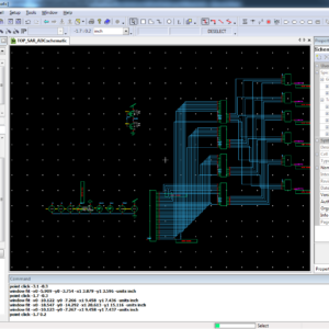
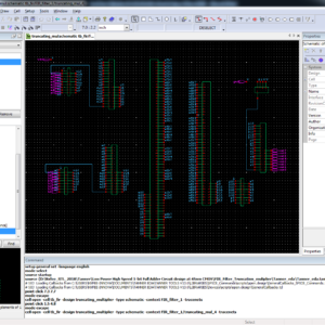
This paper presents a 6-GS/s 6-bit time-interleaved successive approximation register (SAR) analog to digital converter (ADC) realized in 90-nm CMOS. The ADC consists of 32 single SAR-ADCs. The measured effective-number-of-bits (ENOB) at sampling rate of 6.144 GS/s are 5-bit at DC and 3.6-bit at the Nyquist frequency. The power consumption of the ADC-core without I/O’s and 4-to-1 output MUX is 359 mW for an input swing of 1 V peak to peak differential, resulting in a FOM of 4.9 pJ/conv. The proposed design of this Successive approximation register analog to digital converter in Tanner EDA at 65-nm technology and finally proved the comparison of area, power and delay.
List of the following materials will be included with the Downloaded Backup:A Real-Time FHD Learning Based Super Resolution System Without a Frame Buffer
Abstract:
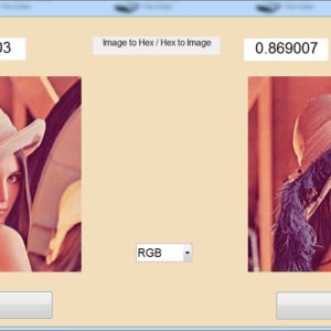
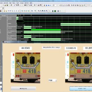
The main aim of the Single image (SR) super-resolution is to generate (HR) high-resolution images from (LR) low-resolution images. This paper briefly presents a concept of real time super resolution method of FHD based image extended and scaling processor. The super resolution system includes three blocks of operations. The first is a low-frequency interpolation stage, where bicubic interpolation is used for reconstructing the low-frequency parts of HR images. The second stage generates high-frequency patches by choosing the highest related pre-trained regression function according to each HR low frequency patch. In the third stage, with the high-frequency information, the low-frequency image patches are enhanced and overlapped to construct the SR result. These operations for gaining a high-frequency result are applied to the Y-luminance channel only, while the high-resolution Cb and Cr channels are generated by bicubic interpolation. The proposed system generates the output image resolution of 1920 X 1080 (FHD) by the input of 800 X 800 image size. The proposed architecture performs an anchored neighborhood regression algorithm that generates a high-resolution image from a low-resolution image input using only numbers of line buffers. Finally, super resolution technique is implemented in VHDL and Synthesized in the XILINX VERTEX-5 FPGA and shown the comparison for power, area and delay reports.
List of the following materials will be included with the Downloaded Backup:Comparative study of 16-order FIR filter design using different multiplication techniques
Abstract:
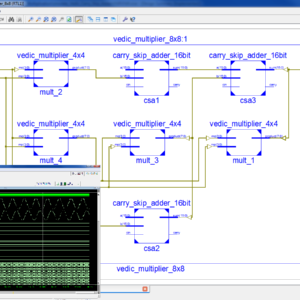
This study represents designing and implementation of a low power and high speed 16 order FIR filter. To optimize filter area, delay and power, different multiplication techniques such as Vedic multiplier, add and shift method and Wallace tree (WT) multiplier are used for the multiplication of filter coefficient with filter input. Various adders such as ripple carry adder, Kogge Stone adder, Brent Kung adder, Ladner Fischer adder and Han Carlson adder are analyzed for optimum performance study for further use in various multiplication techniques along with barrel shifter. Secondly optimization of filter area and delay is done by using add and shift method for multiplication, although it increases power dissipation of the filter. To reduce the complexity of filter, coefficients are represented in canonical signed digit representation as it is more efficient than traditional binary representation. The finite impulse-response (FIR) filter is designed in MATLAB using equiripple method and the same filter is synthesized on Xilinx Spartan 3E XC3S500E target field-programmable gate array device using Very High Speed Integrated Circuit Hardware Description Language (VHDL) subsequently the total on-chip power is calculated in Vivado2014.4. The comparison of simulation results of all the filters show that FIR filter with WT multiplier is the best optimized filter.
List of the following materials will be included with the Downloaded Backup:Design of Power and Area Efficient Approximate Multipliers
Abstract:
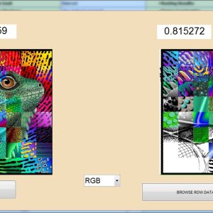
Approximate computing can decrease the design complexity with an increase in performance and power efficiency for error resilient applications. This brief deals with a new design approach for approximation of multipliers. The partial products of the multiplier are altered to introduce varying probability terms. Logic complexity of approximation is varied for the accumulation of altered partial products based on their probability. The proposed approximation is utilized in two variants of 16-bit multipliers. Synthesis results reveal that two proposed multipliers achieve power savings of 72% and 38%, respectively, compared to an exact multiplier. They have better precision when compared to existing approximate multipliers. Mean relative error figures are as low as 7.6% and 0.02% for the proposed approximate multipliers, which are better than the previous works. Performance of the proposed multipliers is evaluated with an image processing application, where one of the proposed models achieves the highest peak signal to noise ratio.
List of the following materials will be included with the Downloaded Backup:Dual Quality 4:2 Compressor for Utilizing in Dynamic Accuracy Configurable Multipliers
Abstract:
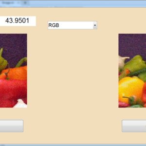
In this paper, we propose four 4:2 compressors, which have the flexibility of switching between the exact and approximate operating modes. In the approximate mode, these dual-quality compressors provide higher speeds and lower power consumptions at the cost of lower accuracy. Each of these compressors has its own level of accuracy in the approximate mode as well as different delays and power dissipations in the approximate and exact modes. Using these compressors in the structures of parallel multipliers provides configurable multipliers whose accuracies (as well as their powers and speeds) may change dynamically during the runtime. The proposed multiplier saves few adder circuits in partial products, and this proposed multiplier is evaluated with an image processing application. In existing thing, to using this multiplier to design image processing evaluation on only luminance based application, but here the proposed work is modified with Gaussian noise reduction with luminance and chrominance based application, this design to implemented in VHDL, and synthesized in Xilinx S6LX9 FPGA and shown the power, area and delay reports.
List of the following materials will be included with the Downloaded Backup:Efficient Super Resolution Algorithm using Overlapping Bi-cubic Interpolation
Abstract:
In practical CCTV applications, there are problems of the camera with low resolution, camera fields of view, and lighting environments. These could degrade the image quality and it is difficult to extract useful information for further processing. Super-resolution techniques have been proposed widely by the researchers. However, many approaches are complex and are difficult to use in practical scenarios. In this paper, we propose an efficient Super-resolution algorithm using overlapping bi-cubic for hardware implementation. Experimental results are verified using processing time and reconstructed images that can be used in real time applications.
List of the following materials will be included with the Downloaded Backup:Energy-Efficient Approximate Multiplier Design using Bit Significance-Driven Logic Compression
Abstract:
Approximate arithmetic has recently emerged as a promising paradigm for many imprecision-tolerant applications. It can offer substantial reductions in circuit complexity, delay and energy consumption by relaxing accuracy requirements. In this paper, we propose a novel energy-efficient approximate multiplier design using a significance-driven logic compression (SDLC) approach. Fundamental to this approach is an algorithmic and configurable lossy compression of the partial product rows based on their progressive bit significance. This is followed by the commutative remapping of the resulting product terms to reduce the number of product rows. As such, the complexity of the multiplier in terms of logic cell counts and lengths of critical paths is drastically reduced. A number of multipliers with different bit-widths (4-bit to 128-bit) are designed in System Verilog and synthesized using Synopsys Design Compiler. Post-synthesis experiments showed that up to an order of magnitude energy savings, and reductions of 65% in critical delay and almost 45% in silicon area can be achieved for a 128-bit multiplier compared to an accurate equivalent. These gains are achieved with low accuracy losses estimated at less than 0.00071 mean relative error. Additionally, we demonstrate the energy-accuracy trade-offs for different degrees of compression, achieved through configurable logic clustering. In evaluating the effectiveness of our approach, a case study image processing application showed up to 68.3% energy reduction with negligible losses in image quality expressed as peak signal-to-noise ratio (PSNR).
List of the following materials will be included with the Downloaded Backup:Energy-Efficient VLSI Realization of Binary64 Division With Redundant Number Systems
Base Paper Abstract:
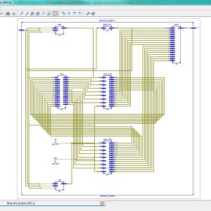
VLSI realizations of digit-recurrence binary division usually use redundant representation of partial remainders and quotient digits. The former allows for fast carry-free computation of the next partial remainder, and the latter leads to less number of the required divisor multiples. In studying the previous relevant works, we have noted that the binary carry save (CS) number system is prevalent in the representation of partial remainders, and redundant high radix representation of quotient digits is popular in order to reduce the cycle count. In this paper, we explore a design space containing four division architectures. These are based on binary CS or radix-16 signed digit (SD) representations of partial remainders. On the other hand, they use full or partial pre computation of divisor multiples. The latter uses smaller multiplexer at the cost two extra adders, where one of the operands is constant within all cycles. The quotient digits are represented by radix-16 [−9,9]SDs. Our synthesis-based evaluation of VLSI realizations of the best previous relevant work and the four proposed designs show reduced power and energy figures in the proposed designs at the cost of more silicon area and delay measures. However, our energy-delay product is 26%–35% less than that of the reference work.
List of the following materials will be included with the Downloaded Backup:High Performance VLSI architecture for M-PSK modems
Abstract:
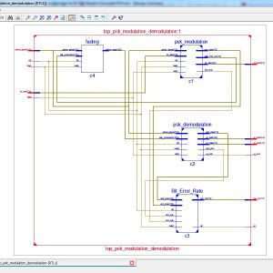
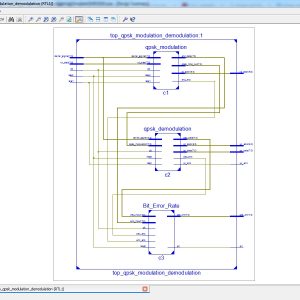
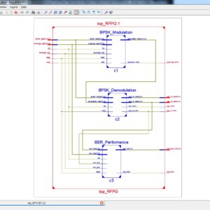
M-PSK (phase shift keying) modulation schemes are used in many high-speed applications like satellite communication, as they are more bandwidth and power efficient compared with other schemes. This study presents very large scale integrated circuits (VLSI) architectures for modulators and demodulators of quadrature phase shift keying (QPSK), 4PSK, 8PSK and 16PSK systems, based on the principle of direct digital synthesis. The proposed modulators do not use any multiplier in contrast to the conventional modulators and hence they are relatively fast and area efficient. Based on the coherent detection technique, this study proposes new demodulation algorithms for 4PSK, 8PSK and 16PSK systems which can be implemented both in analogue and digital domains. This study also presents VLSI architectures for all the proposed algorithms. The proposed architectures are described in VHDL and implemented on Xilinx field programmable gate arrays (FPGAs). The simulation results verify their functional validity and implementation results show the suitability of the proposed architectures for satellite communications.
List of the following materials will be included with the Downloaded Backup:Low Power and High Speed Implementation of FIR filter design using CMOS GDI Truncated Multiplier
Abstract:
The logic size, propagation delay, power of applications, based upon this improvement the adder design logic size will reduced year by year, here a proposed In recent technology of any application, adders is a more priority to do a function and task of arithmetic operation, in crucial this adder based arithmetic operation will decide work of this paper will design using a single bit full adder to design a multiplier. In this multiplier design, adder is a main priority to reduce the arithmetic logic size and increases speed of multiplier, in recent we have lots of multiplier design, Vedic multiplier, Wallace tree multiplier, booth multiplier, approximate multiplier. Here, the proposed work will taken truncated multiplier design, it's because, the truncated multiplier will have a capability to reduced internal and external architecture size in every design, regarding this truncated multiplier will have three options such as rounding, deleting, truncating, here the MSB bits will be truncated and present the output of n x n multiplication will provided only n bit level, using this truncated multiplier the proposed work will designed a 8-Tap FIR(Finite impulse response) filter and shown the efficiency of filter design using this CMOS GDI (Gate Diffusion Input) adder design. This proposed work will design in CMOS Logic gate and which 10-T transistor level of full adders with 90um technology, finally proved the terms of area, delay and power.
List of the following materials will be included with the Downloaded Backup:QPSK Modulator on FPGA
Abstract:
The paper presents the theoretical backgrounds of a QPSK Modulation. The QPSK Modulator is then simulated using Modelsim and Xilinx environment tool for FPGA design as well as implemented on a Spartan 6 LX9 FPGA. The modulator algorithm has been implemented on FPGA using the Verilg HDL language on Xilinx ISE 14.2. The local clock oscillator of the board is 50Mhz which corresponds with a period of 20ns. The frequency of the QPSK carrier is 31,250 kHz and because the QPSK symbol is made of two bits, the output frequency is 62,50kbps. The modulator has been designed and simulated and its performances were evaluated by measurements.
List of the following materials will be included with the Downloaded Backup:Resource Efficient SRAM based Ternary Content Addressable Memory
Abstract:
Static random access memory (SRAM)-based ternary content addressable memory (TCAM) offers TCAM functionality by emulating it with SRAM. However, this emulation suffers from reduced memory efficiency while mapping the TCAM table on SRAM units. This is due to the limited capacity of the physical addresses in the SRAM unit. This brief offers a novel memory architecture called a resource-efficient SRAM-based TCAM (REST), which emulates TCAM functionality using optimal resources. The SRAM unit is divided into multiple virtual blocks to store the address information presented in the TCAM table. This approach virtually increases the overall address space of the SRAM unit, mapping a greater portion of the TCAM table in SRAM and increasing the overall emulated TCAM bits/SRAM at the cost of reduced throughput. A 72 × 28-bit REST consumes only one 36-kbit SRAM and a few distributed RAMs via implementation on a Xilinx Kintex-7 field-programmable gate array. It uses only 3.5% of the memory resources compared with a conventional SRAM-based TCAM (hybrid-partitioned TCAM).
List of the following materials will be included with the Downloaded Backup:RF Power Gating A Low Power Technique for Adaptive Radios
RoBA Multiplier A Rounding Based Approximate Multiplier for High Speed yet Energy Efficient Digital Signal Processing
Abstract:
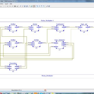
In this paper, we propose an approximate multiplier that is high speed yet energy efficient. The approach is to round the operands to the nearest exponent of two. This way the computational intensive part of the multiplication is omitted improving speed and energy consumption at the price of a small error. The proposed approach is applicable to both signed and unsigned multiplications. We propose three hardware implementations of the approximate multiplier that includes one for the unsigned and two for the signed operations. The efficiency of the proposed multiplier is evaluated by comparing its performance with those of some approximate and accurate multipliers using different design parameters. In addition, the efficacy of the proposed approximate multiplier is studied in two image processing applications, i.e., image sharpening and smoothing.
List of the following materials will be included with the Downloaded Backup:Stochastic Implementation and Analysis of Dynamical Systems Similar to the Logistic Map
Abstract:
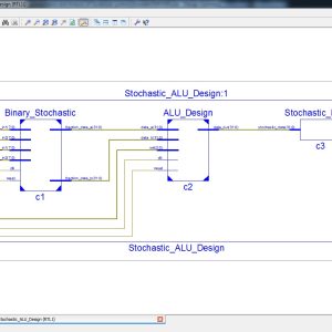
Stochastic computing (SC) is a digital computation approach that operates on random bit streams to perform complex tasks with much smaller hardware, with compared to conventional binary radix approaches. It is characterized by its use of pseudo-random numbers implemented by 0-1 sequences called stochastic numbers (SN) are interpreted as probabilities. Accuracy is usually assumed to depend on the interacting SN being highly independent or uncorrelated in a loosely specified way. This paper introduced a new approach of Stochastic and Analysis of Dynamical digital computation with ALU Design. In existing comparison of Floating point ALU Design is not implemented a Stochastic approach, So here the proposed will design to implemented a Stochastic Computing in ALU Design. In top-down design approach of ALU Design, four arithmetic modules, addition, subtraction, multiplication and division are combined to form a Stochastic ALU Unit. Each module is divided into sub-module with two selection bits are combined to select a particular operation. Each module is independent to each other. This modules are realized and validated using VHDL simulation and synthesized in Xilinx 14.2, finally shown the comparison of Area, Power and Delay.
List of the following materials will be included with the Downloaded Backup:VLSI Implementation of an Edge-Oriented Image Scaling Processor
Abstract:
Image scaling is a very important technique and has been widely used in many image processing applications. In this paper, we present an edge-oriented area-pixel scaling processor. To achieve the goal of low cost, the area-pixel scaling technique is implemented with a low-complexity VLSI architecture in our design. A simple edge catching technique is adopted to preserve the image edge features effectively so as to achieve better image quality. Compared with the previous low-complexity techniques, our method performs better in terms of both quantitative evaluation and visual quality. The seven-stage VLSI architecture of our image scaling processor contains 10.4-K gate counts and yields a processing rate of about 200 MHz by using TSMC 0.18- m technology.
List of the following materials will be included with the Downloaded Backup:IEEE Transactions on VLSI, VLSI IEEE Project, VLSI Low Power Project, VLSI High Speed Project, VLSI Area Efficient Project, Low Cost VLSI Projects, High Speed VLSI Design projects ( CDMA, RTOS, DSP, RF, IF, etc), Low Power VLSI Design projects, Area Efficient VLSI Design projects , Audio processing VLSI Design projects, Signal Processing VLSI Design projects, Image Processing VLSI Design projects, Backend VLSI Design projects ( CMOS, TFET, BisFET, FeFET, etc), Timing & Delay Reduction VLSI Projects, Internet of Things VLSI Projects, Testing, Reliability and Fault Tolerance VLSI Projects, VLSI Applications ( Communicational, Video, Security, Sensor Networks, etc), SOC VLSI Projects, Network on Chip VLSI Projects, Wireless Communication VLSI Projects, VLSI Verifications Projects ( UVM, OVM, VVM, System Verilog.
Provide Wordlwide Online Support
We can provide Online Support Wordlwide, with proper execution, explanation and additionally provide explanation video file for execution and explanations.
24/7 Support Center
NXFEE, will Provide on 24x7 Online Support, You can call or text at +91 9789443203, or email us nxfee.innovation@gmail.com
Terms & Conditions:
Customer are advice to watch the project video file output, and before the payment to test the requirement, correction will be applicable.
After payment, if any correction in the Project is accepted, but requirement changes is applicable with updated charges based upon the requirement.
After payment the student having doubts, correction, software error, hardware errors, coding doubts are accepted.
Online support will not be given more than 3 times.
On first time explanation we can provide completely with video file support, other 2 we can provide doubt clarifications only.
If any Issue on Software license / System Error we can support and rectify that within end of day.
Extra Charges For duplicate bill copy. Bill must be paid in full, No part payment will be accepted.
After payment, to must send the payment receipt to our email id.
Powered by NXFEE INNOVATION, Pondicherry.
Call us today at : +91 9789443203 or Email us at nxfee.innovation@gmail.com
NXFEE Development & Services

Product Categories
- 2014 (11)
- 2015 (39)
- 2016 (30)
- 2017 (16)
- 2018 (17)
- 2019 (42)
- 2020 (29)
- 2021 (17)
- 2022 (23)
- Accessories (45)
- Area Efficient (117)
- High speed VLSI Design (57)
- IEEE (15)
- Image Processing (40)
- Low power VLSI Design (98)
- NOC VLSI Design (2)
- VLSI (251)
- VLSI 2023 (21)
- VLSI 2024 (18)
- VLSI 2025 (32)
- VLSI 2026 (4)
- VLSI Application / Interface and Mini Projects (31)
- VLSI_2023 (15)
Filter by price
Product Status
Sort by producents

Copyright © 2026 Nxfee Innovation.

