IEEE Transactions on VLSI 2016
Following Novelty based Research Projects not yet Published in Any Journal
Customization Available for Journal Publications
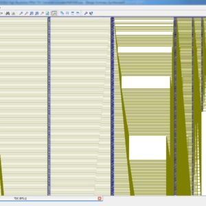
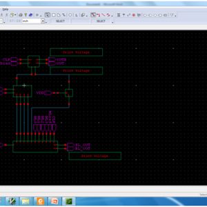
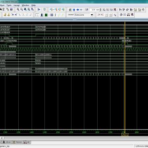
A High Resolution FPGA TDC Converter with 2.5 ps Bin Size and -3.79~6.53 LSB Integral Non linearity
Abstract:
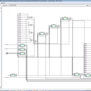
As a traditional digital platform, Field Programmable Gate Array (FPGA) is seldom used for analog applications. Since there is no way to fine tune the gate property or circuit structure, the performance of FPGA analog application is usually inferior to its counterparts based on full-custom or even cell-based design. Nevertheless, a high performance FPGA time-to-digital Converter (TDC) is proposed in this paper to expand the FPGA territory into high-end analog applications. The test time signal is sampled by a serious timing references generated by feeding the original clock into a tapped delay line. According to periodicity, the delays among those timing references are wrapped into a single reference period and the effective TDC resolution can be made much smaller than the clock period to compete even with the state-of the art full-custom TDCs in performance. After measurement, the effective resolution is as fine as 2.5 ps. The corresponding differential nonlinearity (DNL) is -1.90~1.66 LSB and the integral nonlinearity (INL) is -3.79~6.53 LSB only.
List of the following materials will be included with the Downloaded Backup:A Combined Deblocking Filter and SAO Hardware Architecture for HEVC
Abstract:
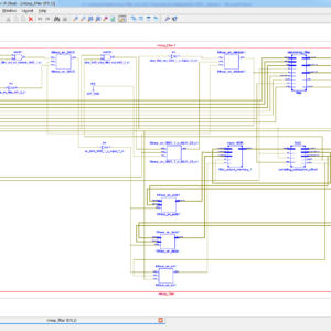
The latest video coding standard high-efficiency video coding (HEVC) provides 50% improvement in coding efficiency compared to H.264/AVC to meet the rising demands for video streaming, better video quality, and higher resolution. The deblocking filter (DF) and sample adaptive offset (SAO) play an important role in the HEVC encoder, and the SAO is newly adopted in HEVC. Due to the high throughput requirement in the video encoder, design challenges such as data dependence, external memory traffic, and on-chip memory area become even more critical. To solve these problems, we first propose an interlacing memory organization on the basis of quarter-LCU to resolve the data dependence between vertical and horizontal filtering of DF. The on-chip SRAM area is also reduced to about 25% on the basis of quarter-LCU scheme without throughput loss. We also propose a simplified bitrate estimation method of rate-distortion cost calculation to reduce the computational complexity in the mode decision of SAO. Our proposed hardware architecture of combined DF and SAO is designed for the HEVC intraencoder, and the proposed simplified bitrate estimation method of SAO can be applied to both intra- and intercoding. As a result, our design can support ultrahigh definition 7680 × 4320 at 40 f/s applications at merely 182 MHz working frequency. Total logic gate count is 103.3 K in 65 nm CMOS process.
List of the following materials will be included with the Downloaded Backup:Design of Low Power High Performance 2-4 and 4-16 Mixed-Logic Line Decoders
Abstract:
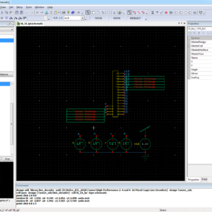
This paper introduces a mixed-logic design method for line decoders, combining transmission gate logic, pass transistor dual-value logic and static CMOS. Two novel topologies are presented for the 2-4 decoders: a 14-transistor topology aiming on minimizing transistor count and power dissipation and a 15-transistor topology aiming on high power delay performance. Both a normal and an inverting decoder are implemented in each case, yielding a total of four new designs. Furthermore, four new 4-16 decoders are designed, by using mixed-logic 2-4 pre decoders combined with standard CMOS post-decoder. All proposed decoders have full swinging capability and reduced transistor count compared to their conventional CMOS counterparts. Finally, a variety of comparative spice simulations at the 32 nm shows that the proposed circuits present a significant improvement in power and delay, outperforming CMOS in almost all cases.
List of the following materials will be included with the Downloaded Backup:HDL-Based Modeling Approach for Digital Simulation of Adiabatic Quantum Flux Parametron Logic
Abstract:
AQFP (adiabatic quantum-flux-parametron) circuits are currently verified by analog-based simulation, which would be an obstacle for large-scale circuits design. In this paper, we present a logic simulation model for AQFP logic. We made a functional model based on a finite-state machine approach using a hardware description language (HDL), which enables the simulation of large-scale AQFP circuits using commercially available logic simulation tools. We have developed a library for logic simulation and implemented an 8-bit carry look-ahead adder, which is composed of over 1000 Josephson junctions (JJs). We also include timing information in our logic simulation models for timing analysis. Since the library is based on a parameterized approach, it can be easily modified for different fabrication technologies and low-level circuit parameters.
List of the following materials will be included with the Downloaded Backup:A Low-Voltage Radiation-Hardened 13T SRAM Bit cell for Ultralow Power Space Applications
Proposed Abstract:
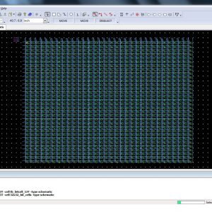
Continuous transistor scaling, coupled with the growing demand for low-voltage, low-power applications, increases the susceptibility of VLSI circuits to soft-errors, especially when exposed to extreme environmental conditions, such as those encountered by space applications. The most vulnerable of these circuits are memory arrays that cover large areas of the silicon die and often store critical data. Radiation hardening of embedded memory blocks is commonly achieved by implementing extremely large bitcells or redundant arrays and maintaining a relatively high operating voltage; however, in addition to the resulting area overhead, this often limits the minimum operating voltage of the entire system leading to significant power consumption. In this paper, we propose the first radiation-hardened static random access memory (SRAM) bitcell targeted at low-voltage functionality, while maintaining high soft-error robustness. A 32×32 bit memory macro was designed and fabricated in a standard 0.13-µm CMOS process, showing full read and write functionality down to the subthreshold voltage of 300 mV. This is achieved with a cell layout that is only 2×larger than a reference 6T SRAM cell drawn with standard design rules. The proposed architecture of this paper is analysis the logic size, area and power consumption using tanner tool.
List of the following materials will be included with the Downloaded Backup:A 65-nm CMOS Constant Current Source With Reduced PVT Variation
Abstract:
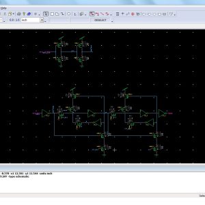
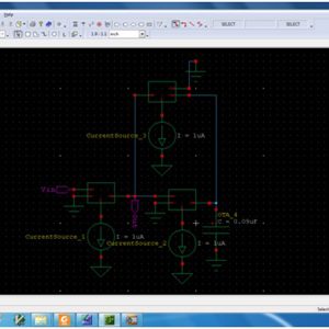
This paper presents a new nanometer-based low-power constant current reference that attains a small value in the total process–voltage–temperature variation. The circuit architecture is based on the embodiment of a process-tolerant bias current circuit and a scaled process-tracking bias voltage source for the dedicated temperature-compensated voltageto-current conversion in a preregulator loop. Fabricated in a UMC 65-nm CMOS process, it consumes 7.18µWwitha1.4V supply. The measured results indicate that the current reference achieves an average temperature coefficient of 119 ppm/°C over 12 samples in a temperature range from−30 °C to 90 °C without any calibration. Besides, a low line sensitivity of 180 ppm/V is obtained. This paper offers a better sensitivity figure of merit with respect to the reported representative counterparts.
List of the following materials will be included with the Downloaded Backup:Design Methodology for Voltage Scaled Clock Distribution Networks
Abstract:
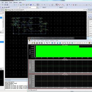
A low-voltage/swing clocking methodology is developed through both circuit and algorithmic innovations. The primary objective is to significantly reduce the power consumed by the clock network while maintaining the circuit performance the same. a novel D-flip-flop (DFF) cell that maximizes power savings by enabling low-voltage/swing operation throughout the entire clock network . In this proposed design of the LSFF is consume the less power compare to existing design. The proposed architecture of this paper is analysis the logic size, area and power consumption using tanner tool.
List of the following materials will be included with the Downloaded Backup:Input Based Dynamic Reconfiguration of Approximate Arithmetic Units for Video Encoding
Abstract:
The field of approximate computing has receivedsignificant attention from the research community in the pastfew years, especially in the context of various signal processingapplications. Image and video compression algorithms, such asJPEG, MPEG, and so on, are particularly attractive candidatesfor approximate computing, since they are tolerant of computingimprecision due to human imperceptibility, which can beexploited to realize highly power-efficient implementations ofthese algorithms. However, existing approximate architecturestypically fix the level of hardware approximation staticallyand are not adaptive to input data. For example, if afixed approximate hardware configuration is used for anMPEG encoder (i.e., a fixed level of approximation), theoutput quality varies greatly for different input videos. Thispaper addresses this issue by proposing a reconfigurableapproximate architecture for MPEG encoders thatoptimizespower consumption with the goal of maintaining a particularPeak Signal-to-Noise Ratio (PSNR) threshold for any video.We propose two heuristics for automaticallytuning the approximation degree of the RABs in thesetwo modules during runtime based on the characteristics of eachindividual video. The proposed architecture of this paper analysis the logic size, area and power consumption using Xilinx 14.2.
List of the following materials will be included with the Downloaded Backup:Low Power Split Radix FFT Processors Using Radix 2 Butterfly Units
Split radix fast Fourier Transform (SRFFT) is an ideal candidate for the implementation of a low power FFT processor, because it has the lowest number of arithmetic operation among all the FFT algorithms. In the design of such processors, an efficient addressing scheme for FFT data as well as twiddle factors is required. The signal flow graph of SRFFT is the same as radix-2 FFT, and therefore, the conventional address generation schemes of FFT data could also be applied to SRFFT. However SRFFT has irregular locations of twiddle factors and forbids the application of radix-2 address generation methods. This brief presents a shared memory low power SRFFT processor architecture. The SRFFT can be computed by using a modified radix-2 butterfly unit. The butterfly unit exploits the multiplier-gating technique to save dynamic power at the expense of using more hardware resources. In addition, two novel address generation algorithm for both the trivial and nontrivial twiddle factors are developed. In this paper We increases the architecture size, of radix-4 and 2048 point complex valued transform, and shown the performance of area, power and delay, and synthesized xilinx FPGA on s6lx16-2csg225.
List of the following materials will be included with the Downloaded Backup:Low Power System for Detection of Symptomatic Patterns in Audio Biological Signals
We present a low-power, efficacious, and scalable system for the detection of symptomatic patterns in biological audio signals. The digital audio recordings of various symptoms, such as cough, sneeze, and so on, are spectrally analyzed using a discrete wavelet transform. Subsequently, we use simple mathematical metrics, such as energy, quasi-average, and coastline parameter for various wavelet coefficients of interest depending on the type of pattern to be detected. Furthermore, a mel-frequency cepstrum-based analysis is applied to distinguish between signals, such as cough and sneeze, which have a similar frequency response and, hence, occur in common wavelet coefficients. Algorithm-circuit codesign methodology is utilized in order to optimize the system at algorithm and circuit levels of design abstraction. This helps in implementing a low-power system as well as maintaining the efficacy of detection. The system is scalable in terms of user specificity as well as the type of signal to be analyzed for an audio symptomatic pattern. The proposed architecture of this paper analysis the logic size, area and power consumption using Xilinx 14.2.
List of the following materials will be included with the Downloaded Backup:Floating Point Butterfly Architecture Based on Binary Signed Digit Representation
Fast Fourier transform (FFT) coprocessor, having a significant impact on the performance of communication systems, has been a hot topic of research for many years. The FFT function consists of consecutive multiply add operations over complex numbers, dubbed as butterfly units. Applying floating-point (FP) arithmetic to FFT architectures, specifically butterfly units, has become more popular recently. It offloads compute-intensive tasks from general-purpose processors by dismissing FP concerns (e.g., scaling and overflow/underflow). However, the major downside of FP butterfly is its slowness in comparison with its fixed-point counterpart. This reveals the incentive to develop a high-speed FP butterfly architecture to mitigate FP slowness. This brief proposes a fast FP butterfly unit using a devised FP fused-dot product-add (FDPA) unit, to compute AB±CD±E, based on binary signed-digit (BSD) representation. The FP three-operand BSD adder and the FP BSD constant multiplier are the constituents of the proposed FDPA unit. A carry-limited BSD adder is proposed and used in the three-operand adder and the parallel BSD multiplier so as to improve the speed of the FDPA unit. Moreover, modified Booth encoding is used to accelerate the BSD multiplier. The synthesis results show that the proposed FP butterfly architecture is much faster than previous counterparts but at the cost of more area. The proposed architecture of this paper analysis the logic size, area and power consumption using Xilinx 14.2.
List of the following materials will be included with the Downloaded Backup:Source Code Error Detection in High Level Synthesis Functional Verification
A dynamic functional verification method that compares untimed simulations versus timed simulations for synthesizable [high-level synthesis (HLS)] behavioral descriptions (ANSI-C) is presented in this paper. This paper proposes a method that automatically inserts a set of probes into the untimed behavioral description. These probes record the status of internal signals of the behavioral description during an initial untimed simulation. These simulation results are subsequently used as golden outputs for the verification of the internal signals during a timed simulation once the behavioral description has been synthesized using HLS. Our proposed method reports any simulation mismatches and accurately pinpoints any discrepancies between the functional Software (SW) simulation and the timed simulation at the original behavioral description (source code). Our method does not only determine where to place the probes, but is also able to insert different type of probes based on the specified HLS synthesis options in order not to interfere with the HLS process, minimizing the total number of probes and the size of the data to be stored in the trace file in order to minimize the running time. Results show that our proposed method is very effective and extremely simple to use as it is fully automated using Xilinx 14.2.
List of the following materials will be included with the Downloaded Backup:
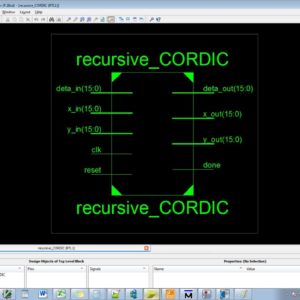
Concept Design and Implementation of Reconfigurable CORDIC
This brief presents the key concept, design strategy, and implementation of reconfigurable coordinate rotation digital computer (CORDIC) architectures that can be configured to operate either for circular or for hyperbolic trajectories in rotation as well as vectoring-modes. It can, therefore, be used to perform all the functions of both circular and hyperbolic CORDIC. We propose three reconfigurable CORDIC designs: 1) a reconfigurable rotation-mode CORDIC that operates either for circular or for hyperbolic trajectory; 2) a reconfigurable vectoring-mode CORDIC for circular and hyperbolic trajectories; and 3) a generalized reconfigurable CORDIC that can operate in any of the modes for both circular and hyperbolic trajectories. The reconfigurable CORDIC can perform the computation of various trigonometric and exponential functions, logarithms, square-root, and so on of circular and hyperbolic CORDIC using either rotation-mode or vectoring-mode CORDIC in one single circuit. It can be used in digital synchronizers, graphics processors, scientific calculators, and so on. It offers substantial saving of area complexity over the conventional design for reconfigurable applications. The proposed architecture of this paper analysis the logic size, area and power consumption using Xilinx 14.2.
List of the following materials will be included with the Downloaded Backup:
Low Power FPGA Design Using Memoization Based Approximate Computing
Field-programmable gate arrays (FPGAs) are increasingly used as the computing platform for fast and energy efficient execution of recognition, mining, and search applications. Approximate computing is one promising method for achieving energy efficiency. Compared with most prior works on approximate computing, which target approximate processors and arithmetic blocks, this paper presents an approximate computing methodology for FPGA-based design. It studies memoization as a method for approximation on FPGA and analyzes different architectural and design parameters that should be considered. The proposed design flow leverages on high-level synthesis to enable memoization-based microarchitecture generation, thus also facilitating a C-to-register-transfer-level synthesis. When compared with the previous approaches of bit-width truncation and approximate multipliers, memoization-based approximate computation on FPGA achieves a significant dynamic power saving (around 20%) with very small area overhead (<5%) and better power-to-signal noise ratio values for the studied image processing benchmarks. The proposed architecture of this paper is verified using vivado HLS..
List of the following materials will be included with the Downloaded Backup:
A High Speed FPGA Implementation of an RSD Based ECC Processor
In this paper, an exportable application-specific instruction-set elliptic curve cryptography processor based on redundant signed digit representation is proposed. The processor employs extensive pipelining techniques for Karatsuba–Ofman method to achieve high throughput multiplication. Furthermore, an efficient modular adder without comparison and a highthrough put modular divider, which results in a short datapath for maximized frequency, are implemented. The processor supports the recommended NIST curve P256 and is based on an extended NIST reduction scheme. The proposed architecture of this paper analysis the logic size, area and power consumption using Xilinx 14.2.
List of the following materials will be included with the Downloaded Backup:
A Multiuser Detection Algorithm in the Uplink SCFDMA System for Green Communication network
In mobile network the multiuser detection mostly in 5G networks with using communication of CDMA, SC-FDMA, UTMS, EDGE, FDMA, WI-MAX etc,. Here SC-FDMA (Single Carrier FDMA) plays major role in 5G networks even the performance of improving Low Power Consumption in Low Peak to average ratio of RF Signal Transmission. The iteration of signal transmission in the same manner of Multi User SC-FDMA requires traditional parallel and serial interference cancellation algorithm for achieving the result in large, where the algorithm is consumed to be low power consumption. In the same manner to eliminate the Multiple access RF communication, here the proposed algorithm is introduces in named Optical Weighted Parallel Interference Cancellation (OWPIC). As a result to implement the SC-FDMA with high precision then traditional Parallel Interference Cancellation(PIC) with Multi User SC-FDMA using OWPIC, and also implement this architecture in FPGA (S5LX9) and finally analysis the logic size, low power consumption, high frequency interference, radio signal interference.
List of the following materials will be included with the Downloaded Backup:
A Computation and Energy Reduction Technique for HEVC Discrete Cosine Transform
In this paper, a novel computation and energy reduction technique for High Efficiency Video Coding (HEVC) Discrete Cosine Transform (DCT) for all Transform Unit (TU) sizes is proposed. The proposed technique reduces the computational complexity of HEVC DCT significantly at the expense of slight decrease in PSNR and slight increase in bit rate by only calculating several pre-determined low frequency coefficients of TUs and assuming that the remaining coefficients are zero. It reduced the execution time of HEVC HM software encoder up to 12.74%, and it reduced the execution time of DCT operations in HEVC HM software encoder up to 37.27%. In this paper, a low energy HEVC 2D DCT hardware for all TU sizes is also designed and implemented using Verilog HDL. The proposed hardware, in the worst case, can process 53 Ultra HD (7680x4320) video frames per second. The proposed technique reduced the energy consumption of this hardware up to 18.9%. Therefore, it can be used in portable consumer electronics products that require a real-time HEVC encoder. The proposed architecture of this paper analysis the logic size, area and power consumption using Xilinx 14.2.
List of the following materials will be included with the Downloaded Backup:High Speed Low Power and Highly Reliable Frequency Multiplier for DLL Based Clock Generator
To propose a novel frequency multiplier with high-speed, low-power, and highly reliable design for a delay-locked loop-based clock generator to generate a multiplied clock with a high frequency and wide frequency range. The proposed edge combiner achieves a high-speed and highly reliable operation using a hierarchical structure and an overlap canceller. In addition, by applying the logical effort to the pulse generator and multiplication-ratio control logic design, the proposed frequency multiplier minimizes the delay difference between positive- and negative-edge generation paths, which causes a deterministic jitter. Finally, a numerical analysis is performed to analyze and compare the performance of the proposed frequency multiplier with that of previous frequency multipliers. The proposed frequency multiplier is fabricated using a 0.13-µm CMOS process technology, and has the multiplication ratios of 1, 2, 4, 8, and 16, and an output range of 50 MHz–3.3 GHz. The frequency multiplier achieves power consumption is 17.49mW. The proposed architecture of this paper is analysis the logic size, area and power consumption using tanner tool.
List of the following materials will be included with the Downloaded Backup:
Full Swing Local Bitline SRAM Architecture Based on the 22 nm FinFET Technology for Low Voltage Operation
The previously proposed average-8T static random access memory (SRAM) has a competitive area and does not require a write-back scheme. In the case of an average-8T SRAM architecture, a full-swing local bitline (BL) that is connected to the gate of the read buffer can be achieved with a boosted wordline (WL) voltage. However, in the case of an average-8T SRAM based on an advanced technology, such as a 22-nm FinFET technology, where the variation in threshold voltage is large, the boosted WL voltage cannot be used, because it degrades the read stability of the SRAM. Thus, a full-swing local BL cannot be achieved, and the gate of the read buffer cannot be driven by the full supply voltage (VDD), resulting in a considerably large read delay. To overcome the above disadvantage, in this paper, a differential SRAM architecture with a full-swing local BL is proposed. In the proposed SRAM architecture, full swing of the local BL is ensured by the use of cross-coupled pMOSs, and the gate of the read buffer is driven by a full VDD, without the need for the boosted WL voltage. Various configurations of the proposed SRAM architecture, which stores multiple bits, are analyzed in terms of the minimum operating voltage and area per bit. The proposed SRAM that stores four bits in one block can achieve a minimum voltage of 0.42 V and a read delay that is 62.6 times lesser than that of the average-8T SRAM based on the 22-nm FinFET technology. The proposed architecture of this paper is analysis the area and power consumption using tanner tool.
List of the following materials will be included with the Downloaded Backup:
A Fully Digital Front End Architecture for ECG Acquisition System with 0.5 V Supply
This paper presents a new power-efficient electrocardiogram acquisition system that uses a fully digital architecture to reduce the power consumption and chip area. The proposed architecture is compatible with digital CMOS technology and is capable of operating with a low supply voltage of 0.5 V. In this architecture, no analog block, e.g., low-noise amplifier (LNA), and filters, and no passive elements, such as ac coupling capacitors, are used. A moving average voltage-to time converter is used, which behaves instead of the LNA and anti-aliasing filter. A digital feedback loop is employed to cancel the impact of the dc offset on the circuit, which eliminates the need for coupling capacitors. The proposed architecture of this paper area and power consumption is analysis using tanner tool.
List of the following materials will be included with the Downloaded Backup:Low Power ECG Based Processor for Predicting Ventricular Arrhythmia
This paper presents the design of a fully integrated electrocardiogram (ECG) signal processor (ESP) for the prediction of ventricular arrhythmia using a unique set of ECG features and a naive Bayes classifier. Real-time and adaptive techniques for the detection and the delineation of the P-QRS-T waves were investigated to extract the fiducial points. We are also detecting the all interval in the ECG signal and compare the stored record for Ventricular Arrhythmia with also energy/area architecture design. The proposed architecture of this paper analysis the logic size, area and power consumption using Xilinx 14.2.
List of the following materials will be included with the Downloaded Backup:
A New Parallel VLSI Architecture for Real-time Electrical Capacitance Tomography
This paper presents a fixed-point reconfigurable parallel VLSI hardware architecture for real-time Electrical Capacitance Tomography (ECT). Another FPGA module performs the inverse steps of the tomography algorithm. A dual port built-in memory banks store the sensitivity matrix, the actual value of the capacitances, and the actual image with RGB format. A two dimensional (2D) core multiprocessing elements (PE) engine intercommunicates with these memory banks via parallel buses. We are focus only on the FPGA module because the design is decide the power consumption and cost. The proposed architecture of this paper analysis the logic size, area and power consumption using Xilinx 14.2.
List of the following materials will be included with the Downloaded Backup:40-Gb/s 0.7-V 2:1 MUX and 1:2 DEMUX with Transformer-Coupled Technique for SerDes Interface
This paper explores the use of transformer-coupled (TC) technique for the 2:1 MUX and the 1:2 DEMUX to serialize-and-deserialize (SerDes) high-speed data sequence. The widely used current-mode logic (CML) designs of latch and multiplexer/demultiplexer (MUX/DEMUX) are replaced by the proposed TC approach to allow the more headroom and to lower the power consumption. Through the stacked transformer, the input clock pulls down the differential source voltage of the TC latch and the TC multiplexer core while alternating between the two-phase operations. With the enhanced drain-source voltage, the TC design attracts more drain current with less width-to-length ratio of NMOS than that of the CML counterpart. The source-offset voltage is decreased so that the supply voltage can be reduced. The lower supply voltage improves the power consumption and facilitates the integration with low voltage supply SerDes interface. The MUX and the DEMUX chips are fabricated in 65-nm standard CMOS process and operate at 0.7-V supply voltage. The chips are measured up to 40-Gb/s with sub-hundred milliwatts power consumption.
List of the following materials will be included with the Downloaded Backup:
Frequency-Boost Jitter Reduction for Voltage-Controlled Ring Oscillators
Ring oscillators (ROs) are popular due to their small area, modest power, wide tuning range, and ease of scaling with process technology. However, their use in many applications is limited due to poor phase noise and jitter performance. Thermal noise and flicker noise contribute jitter that decreases inversely with oscillation frequency. This paper describes a frequency boost technique to reduce jitter in ROs. We boost the internal oscillation frequency and introduce a frequency divider following the oscillator to maintain the desired output frequency. This approach offers reduced jitter as well as the opportunity to trade off output jitter with power for dynamic performance management. The oscillator has 32 operating modes, corresponding to different values for the ring size and frequency division. In a 0.5-µm CMOS process, the highest oscillation frequency achieved is 25 MHz with a root-mean-square period jitter of 54 ps and a power consumption of 817 µW at 5 V supply. A jitter model for current-starved oscillators was derived and verified by measurement; a direct relationship between oscillation frequency and jitter was derived and measured. Compared with other oscillators, this design achieves the highest performance in terms of jitter per unit interval and figure-of-merit. The performance is expected to improve in more advanced technologies. The results are summarized to offer design guidance based on the frequency boost technique. The proposed architecture of this paper area and power consumption analysis using tanner tool.
List of the following materials will be included with the Downloaded Backup:
Low-Energy Power-ON-Reset Circuit for Dual Supply SRAM
Design of a low-energy power-ON reset (POR) circuit is proposed to reduce the energy consumed by the stable supply of the dual supply static random access memory (SRAM), as the other supply is ramping up. The proposed POR circuit, when embedded inside dual supply SRAM, removes its ramp-up constraints related to voltage sequencing and pin states. The circuit consumes negligible energy during ramp-up, does not consume dynamic power during operations, and includes hysteresis to improve noise immunity against voltage fluctuations on the power supply. The POR circuit, designed in the 40-nm CMOS technology within 10.6-µm2 area, enabled 27× reduction in the energy consumed by the SRAM array supply during periphery power-up in typical conditions. The proposed architecture of this paper area and power consumption analysis using tanner tool.
List of the following materials will be included with the Downloaded Backup:
Low Power Variation Tolerant Nonvolatile Lookup Table Design
Emerging nonvolatile memories (NVMs), such as MRAM, PRAM, and RRAM, have been widely investigated to replace SRAM as the configuration bits in field-programmable gate arrays (FPGAs) for high security and instant power ON. However, the variations inherent in NVMs and advanced logic process bring reliability issue to FPGAs. This brief introduces a low-power variation-tolerant nonvolatile lookup table (nvLUT) circuit to overcome the reliability issue. Because of large ROFF/RON, 1T1R RRAM cell provides sufficient sense margin as a configuration bit and a reference resistor. A single-stage sense amplifier with voltage clamp is employed to reduce the power and area without impairing the reliability. Matched reference path is proposed to reduce the parasitic RC mismatch for reliable sensing. Evaluation shows that 22% reduction in delay, 38% reduction in power, and the tolerance of variations of 2.5× typical RON or ROFF in reliability are achieved for proposed nvLUT with six inputs. The proposed architecture of this paper area and power consumption analysis using tanner tool.
List of the following materials will be included with the Downloaded Backup:
A 0.1–3.5-GHz Duty-Cycle Measurement and Correction Technique in 130-nm CMOS
A duty-cycle correction technique using a novel pulse width modification cell is demonstrated across a frequency range of 100 MHz–3.5 GHz. The technique works at frequencies where most digital techniques implemented in the same technology node fail. An alternative method of making time domain measurements such as duty cycle and rise/fall times from the frequency domain data is introduced. The data are obtained from the equipment that has significantly lower bandwidth than required for measurements in the time domain. An algorithm for the same has been developed and experimentally verified. The correction circuit is implemented in a 0.13-µm CMOS technology and occupies an area of 0.011 mm2. It corrects to a residual error of less than 1%. The extent of correction is limited by the technology at higher frequencies. The proposed architecture of this paper area and power consumption analysis using tanner tool.
List of the following materials will be included with the Downloaded Backup:
OTA-Based Logarithmic Circuit for Arbitrary Input Signal and Its Application
In this paper, a new design procedure has been proposed for realization of logarithmic function via three phases: 1) differentiation; 2) division; and 3) integration for any arbitrary analog signal. All the basic building blocks, i.e., differentiator, divider, and integrator, are realized by operational transconductance amplifier, a current mode device. Realization of exponential, power law and hyperbolic function as the design examples claims that the proposed synthesis procedure has the potential to design a log-based nonlinear system in a systematic and hierarchical manner. The proposed architecture of this paper area and power consumption analysis using tanner tool.
List of the following materials will be included with the Downloaded Backup:In-Field Test for Permanent Faults in FIFO Buffers of NoC Routers
Abstract:
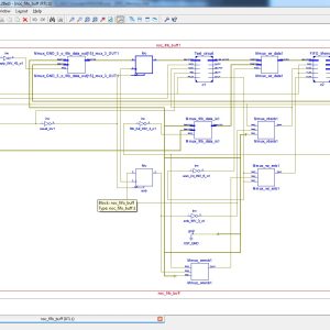
This brief proposes an on-line transparent test technique for detection of latent hard faults which develop in first input first output buffers of routers during field operation of NoC. The technique involves repeating tests periodically to prevent accumulation of faults. A prototype implementation of the proposed test algorithm has been integrated into the router-channel interface and on-line test has been performed with synthetic self-similar data traffic. The performance of the NoC after addition of the test circuit has been investigated in terms of throughput while the area overhead has been studied by synthesizing the test hardware. In addition, an on-line test technique for the routing logic has been proposed which considers utilizing the header flits of the data traffic movement in transporting the test patterns.
List of the following materials will be included with the Downloaded Backup:Low-Cost High-Performance VLSI Architecture for Montgomery Modular Multiplication
Source Code : VHDL & VERILOG HDL
Abstract: This paper proposes a simple and efficient Montgomery multiplication algorithm such that the low-costand high-performance Montgomery modular multiplier can be implemented accordingly. The proposed multiplier output data with representation and uses only one parallel prefix adder to avoid a carry propagation and reduce the area, power and delay, and also increasing the speed. Mainly the usage of parallel prefix adder is to reduce the significant delay reduction and area × time2 improvements, all this at the cost of higher power consumption, which is the main reason preventing the use of parallel-prefix adders to achieve high-speed reverse converters in nowadays systems. Hence, to solve the high power consumption problem, novel specific hybrid parallel-prefix-based adder components those provide better trade-off between delay and power consumption. As a result, the extra clock cycles for operand pre-computation and format conversion can be hidden and high throughput can be obtained. Experimental results show that the proposed Montgomery modular multiplier can achieve higher performance and significant area–time product improvement when compared with previous designs. Using VHDL to design the RTL, and the result to be shown in Xilinx 14.2 with Power consumption and area reduction.
List of the following materials will be included with the Downloaded Backup:
IEEE Transactions on VLSI, VLSI IEEE Project, VLSI Low Power Project, VLSI High Speed Project, VLSI Area Efficient Project, Low Cost VLSI Projects, High Speed VLSI Design projects ( CDMA, RTOS, DSP, RF, IF, etc), Low Power VLSI Design projects, Area Efficient VLSI Design projects , Audio processing VLSI Design projects, Signal Processing VLSI Design projects, Image Processing VLSI Design projects, Backend VLSI Design projects ( CMOS, TFET, BisFET, FeFET, etc), Timing & Delay Reduction VLSI Projects, Internet of Things VLSI Projects, Testing, Reliability and Fault Tolerance VLSI Projects, VLSI Applications ( Communicational, Video, Security, Sensor Networks, etc), SOC VLSI Projects, Network on Chip VLSI Projects, Wireless Communication VLSI Projects, VLSI Verifications Projects ( UVM, OVM, VVM, System Verilog.
Provide Wordlwide Online Support
We can provide Online Support Wordlwide, with proper execution, explanation and additionally provide explanation video file for execution and explanations.
24/7 Support Center
NXFEE, will Provide on 24x7 Online Support, You can call or text at +91 9789443203, or email us nxfee.innovation@gmail.com
Terms & Conditions:
Customer are advice to watch the project video file output, and before the payment to test the requirement, correction will be applicable.
After payment, if any correction in the Project is accepted, but requirement changes is applicable with updated charges based upon the requirement.
After payment the student having doubts, correction, software error, hardware errors, coding doubts are accepted.
Online support will not be given more than 3 times.
On first time explanation we can provide completely with video file support, other 2 we can provide doubt clarifications only.
If any Issue on Software license / System Error we can support and rectify that within end of day.
Extra Charges For duplicate bill copy. Bill must be paid in full, No part payment will be accepted.
After payment, to must send the payment receipt to our email id.
Powered by NXFEE INNOVATION, Pondicherry.
Call us today at : +91 9789443203 or Email us at nxfee.innovation@gmail.com
NXFEE Development & Services

Product Categories
- 2014 (11)
- 2015 (39)
- 2016 (30)
- 2017 (16)
- 2018 (17)
- 2019 (42)
- 2020 (29)
- 2021 (17)
- 2022 (23)
- Accessories (47)
- Area Efficient (117)
- High speed VLSI Design (57)
- IEEE (15)
- Image Processing (40)
- Low power VLSI Design (99)
- NOC VLSI Design (2)
- VLSI (253)
- VLSI 2023 (21)
- VLSI 2024 (18)
- VLSI 2025 (33)
- VLSI 2026 (4)
- VLSI Application / Interface and Mini Projects (31)
- VLSI_2023 (15)
Filter by price
Product Status
Sort by producents

Copyright © 2026 Nxfee Innovation.

