NXFEE – High Speed VLSI Design
A High Speed FPGA Implementation of an RSD Based ECC Processor
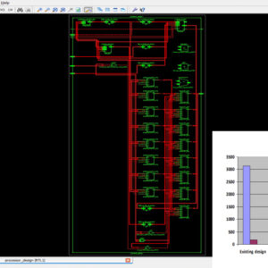
In this paper, an exportable application-specific instruction-set elliptic curve cryptography processor based on redundant signed digit representation is proposed. The processor employs extensive pipelining techniques for Karatsuba–Ofman method to achieve high throughput multiplication. Furthermore, an efficient modular adder without comparison and a highthrough put modular divider, which results in a short datapath for maximized frequency, are implemented. The processor supports the recommended NIST curve P256 and is based on an extended NIST reduction scheme. The proposed architecture of this paper analysis the logic size, area and power consumption using Xilinx 14.2.
List of the following materials will be included with the Downloaded Backup:
A High-Speed FPGA-based True Random Number Generator using Metastability with Clock Managers
Base Paper Abstract:
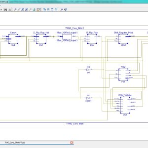
True random number generators (TRNGs) are fundamentals in many important security applications. Though they exploit randomness sources that are typical of the analog domain, digital-based solutions are strongly required especially when they have to be implemented on Field Programmable Gate Array (FPGA)-based digital systems. This paper describes a novel methodology to easily design a TRNG on FPGA devices. It exploits the runtime capability of the Digital Clock Manager (DCM) hardware primitives to tune the phase shift between two clock signals. The presented auto-tuning strategy automatically sets the phase difference of two clock signals in order to force on one or more flip-flops (FFs) to enter the metastability region, used as a randomness source. Moreover, a novel use of the fast carry-chain hardware primitive is proposed to further increase the randomness of the generated bits. Finally, an effective on-chip post-processing scheme that does not reduce the TRNG throughput is described. The proposed TRNG architecture has been implemented on the Xilinx Zynq XC7Z020 System on Chip (SoC). It passed all the National Institute of Standards and Technology (NIST) SP 800-22 statistical tests with a maximum throughput of 300×106 bit per second. The latter is considerably higher than the throughput of other previously published DCMbased TRNGs.
List of the following materials will be included with the Downloaded Backup:A High-Throughput VLSI Architecture for Hard and Soft SC-FDMA MIMO Detectors
Abstract:
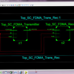
A novel low-complexity multiple-input multiple-output (MIMO) detector tailored for single-carrier frequency division-multiple access (SC-FDMA) systems, suitable for efficient hardware implementations. The proposed detector starts with an initial estimate of the transmitted signal based on a minimum mean square error (MMSE) detector. Subsequently, it recognizes less reliable symbols for which more candidates in the constellation are browsed to improve the initial estimate. The proposed architecture of this paper analysis the logic size, area and power consumption using Xilinx 14.2.
List of the following materials will be included with the Downloaded Backup:A Highly Efficient Conditional Feed through Pulsed Flip Flop for High Speed Applications
Abstract:
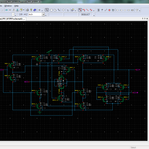
A novel type of highly efficient conditional feed through pulse-triggered flip-flop (P-FF) is proposed and demonstrated. The data-to-output (D-to-Q) delay in this circuit was highly optimized using pre discharging and conditional signal feed through schemes. Power consumption was also reduced using a shared pulse generator and an output feedback-controlled conditional keeper, which diminished the floating status of the internal node. The driving strength of this design was further enhanced by including an additional pull-down path at the output node. Various post layout simulation results applied to 16-nm Fin FET technology demonstrated a higher energy efficiency (at all input data toggle rates) for the proposed topology than comparable P-FF devices. Notably, the proposed model achieved a 62% D-to-Q delay reduction, compared to a transmission gate FF, outperforming the device by more than 66% in terms of power efficiency and 87% in energy efficiency (at a 50% input data toggle rate). Improvements were even more significant in comparison with other conventional P-FFs. These results suggest the proposed design to be a viable new option for high-efficiency sequential elements in high-speed applications.
List of the following materials will be included with the Downloaded Backup:A Low Complexity I/Q Imbalance Calibration Method for Quadrature Modulator
Abstract:
This brief presents a low-complexity I/Q (in-phase and quadrature components) imbalance calibration method for the transmitter using quadrature modulation. Impairments in analog quadrature modulator have a deleterious effect on the signal fidelity. Among the critical impairments, I/Q imbalance (gain and phase mismatches) deteriorates the residual sideband performance of the analog quadrature modulator degrading the error vector magnitude. Based on the theoretical mismatch analysis of the quadrature modulator, we propose a low-complexity I/Q imbalance extraction algorithm. After the parameter extraction, the transmitter is calibrated by imposing the counter imbalanced mismatch of the transmitter through the digital baseband. In comparison with existing I/Q imbalance calibration methods, the novelty of the proposed method lies in that: 1) only three spectrum measurements of the device-under-test are needed for extraction and calibration of gain and phase mismatches; 2) due to the blind nature of the calibration algorithm, the proposed approach can be readily applicable to an existing I/Q transmitter; 3) no extra hardware that degrades the calibration accuracy is required; and 4) due to the non-iterative nature, the proposed method is faster and computationally more efficient than previously published methods.
List of the following materials will be included with the Downloaded Backup:A Multiuser Detection Algorithm in the Uplink SCFDMA System for Green Communication network
In mobile network the multiuser detection mostly in 5G networks with using communication of CDMA, SC-FDMA, UTMS, EDGE, FDMA, WI-MAX etc,. Here SC-FDMA (Single Carrier FDMA) plays major role in 5G networks even the performance of improving Low Power Consumption in Low Peak to average ratio of RF Signal Transmission. The iteration of signal transmission in the same manner of Multi User SC-FDMA requires traditional parallel and serial interference cancellation algorithm for achieving the result in large, where the algorithm is consumed to be low power consumption. In the same manner to eliminate the Multiple access RF communication, here the proposed algorithm is introduces in named Optical Weighted Parallel Interference Cancellation (OWPIC). As a result to implement the SC-FDMA with high precision then traditional Parallel Interference Cancellation(PIC) with Multi User SC-FDMA using OWPIC, and also implement this architecture in FPGA (S5LX9) and finally analysis the logic size, low power consumption, high frequency interference, radio signal interference.
List of the following materials will be included with the Downloaded Backup:
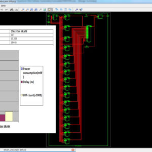
A Novel Quantum Dot Cellular Automata X bit × 32 bit SRAM
Application of quantum-dot cellular automata (QCA) technology as an alternative to CMOS technology on the nanoscale has a promising future; QCA is an interesting technology for building memory. The proposed design and simulation of a new memory cell structure based on QCA with a minimum delay, area, and complexity is presented to implement a static random access memory (SRAM). This paper presents the design and simulation of a 16-bit × 32-bit SRAM with a new structure in QCA. Since QCA is a pipeline, this SRAM has a high operating speed. The 16-bit × 32-bit SRAM has a new structure with a 32-bit width designed and implemented in QCA. It has the ability of a conventional logic SRAM that can provide read/write operations frequently with minimum delay. The 16-bit × 32-bit SRAM is generalized and an n × 16-bit × 32-bit SRAM is implemented in QCA. Novel 16-bit decoders and multiplexers (MUXs) in QCA are presented that have been designed with a minimum number of majority gates and cells. The new SRAM, decoders, and MUXs are designed, implemented, and simulated in QCA using a signal distribution network to avoid the coplanar problem of crossing wires. The QCA-based SRAM cell was compared with the SRAM cell based on CMOS. Results show that the proposed SRAM is more efficient in terms of area, complexity, clock frequency, latency, throughput, and power consumption.
List of the following materials will be included with the Downloaded Backup:
A Pipelined Reduced Complexity Two Stages Parallel LMS Structure for Adaptive Beam forming
Base Paper Abstract:
In this paper, we propose a reduced complexity parallel least mean square structure (RC-pLMS) for adaptive beamforming and its pipelined hardware implementation. RC-pLMS is formed by two least mean square (LMS) stages operating in parallel (pLMS), where the overall error signal is derived as a combination of individual stage errors. The pLMS is further simplified to remove the second independent set of weights resulting in a reduced complexity pLMS (RC-pLMS) design. In order to obtain a pipelined hardware architecture of our proposed RC-pLMS algorithm, we applied the delay and sum relaxation technique (DRC-pLMS). Convergence, stability and quantization effect analysis are performed to determine the upper bound of the step size and assess the behavior of the system. Computer simulations demonstrate the outstanding performance of the proposed RC-pLMS in providing accelerated convergence and reduced error floor while preserving a LMS identical O(N) complexity, for an antenna array of N elements. Synthesis and implementation results show that the proposed design achieves a significant increase in the maximum operating frequency over other variants with minimal resource usage. Additionally, the resulting beam radiation pattern show that the finite precision DRC-pLMS implementation presents similar behavior of the infinite precision theoretical results.
List of the following materials will be included with the Downloaded Backup:A VLSI-Based Hybrid ECG Compression Scheme for Wearable Sensor Node
Base Paper Abstract:
During smart long-term monitoring of any biomedical signal in wireless body area networks, wearable sensor nodes generate and transmit a large amount of data, increasing transmission power consumption. In order to reduce data storage and power consumption, a lossless data compression technique for an electrocardiogram signal monitoring system is presented in this letter. For this, a hybrid lossless compression algorithm based on Run-length coding and Golomb–Rice coding is proposed to enhance the bit compressing rate. The lossless encoding scheme is implemented on the MIT-BIH arrhythmia database, achieving a compression ratio of 2.91. A VLSI-based architecture of the data compression algorithm is implemented in 90nm CMOS technology that consumes power of 18.78 µW at 100 MHz operating frequency and 1.2 V supply voltage, occupying an area of 0.0051 mm2.
List of the following materials will be included with the Downloaded Backup:An Analog LO Harmonic Suppression Technique for SDR Receivers
Abstract:
A low-complexity analog technique to suppress the local oscillator (LO) harmonics in software-defined radios is presented. Accurate mathematical analyses show that an effective attenuation of the LO harmonics is achieved by modulating the transconductance of the low-noise transconductance amplifier (LNTA) with a raised-cosine signal. This modulation is performed through the bias network of a cascode device with a negligible increase in the LNTA noise figure. The proposed technique results in a notch at the third harmonic and at least 36 dB of attenuation at the fifth and the seventh harmonics. Experimental results in 130-nm CMOS and post layout simulation results in 65-nm CMOS verify the proper functionality of the proposed technique and the accuracy of the proposed analyses
List of the following materials will be included with the Downloaded Backup:An Efficient VLSI Architecture for Convolution Based DWT Using MAC
Abstract:
The modern real time applications related to image processing and etc., demand high performance discrete wavelet transform (DWT). This paper proposes the floating point multiply accumulate circuit (MAC) based 1D/2D-DWT, where the MAC is used to find the outputs of high/low pass FIR filters. The proposed technique is implemented with 45 nm CMOS technology and the results are compared with various existing techniques. The proposed 8 × 8-point floating point 2-levels 2D-DWT achieves 27.6% and 83.7% of reduction in total area and net power respectively as compared with existing DWT.
List of the following materials will be included with the Downloaded Backup:An Efficient VLSI Architecture of a Reconfigurable Pulse Shaping FIR Interpolation
This brief proposes a two-step optimization technique for designing a reconfigurable VLSI architecture of an interpolation filter for multi-standard digital up converter (DUC) to reduce the power and area consumption. The proposed technique initially reduces the number of multiplications per input sample and additions per input sample by 83% in comparison with individual implementation of each standard’s filter while designing a root-raised-cosine finite-impulse response filter for multi-standard DUC for three different standards. In the next step, a 2-bit binary common sub-expression (BCS)-based BCS elimination algorithm has been proposed to design an efficient constant multiplier, which is the basic element of any filter. This technique has succeeded in reducing the area and power usage by 41% and 38%, respectively, along with 36% improvement in operating frequency over a 3-bit BCS-based technique reported earlier, and can be considered more appropriate for designing the multi-standard DUC. The proposed architecture of this paper analysis the logic size, area and power consumption using Xilinx 14.2.
List of the following materials will be included with the Downloaded Backup:
Approximate Pruned and Truncated Haar Discrete Wavelet Transform VLSI Hardware for Energy-Efficient ECG Signal Processing
Abstract:
The approximate computing paradigm emerged as a key alternative for trading off accuracy and energy efficiency. Error-tolerant applications, such as multimedia and signal processing, can process the information with lower-than-standard accuracy at the circuit level while still fulfilling a good and acceptable service quality at the application level. The automatic detection of R-peaks in an electrocardiogram (ECG) signal is the essential step preceding ECG processing and analysis. The Haar discrete wavelet transform (HDWT) is a low-complexity pre-processing filter suitable to detect ECG R-peaks in embedded systems like wearable devices, which are incredibly energy constrained. This work presents an approximate HDWT hardware architecture for ECG processing at very high energy efficiency. Our best-proposal employing pruning within the approximate HDWT hardware architecture requires just seven additions. The use of a truncation technique to improve energy efficiency is also investigated herein by observing the evolution of the signal-to-noise ratio and the ultimate impact in the ECG peak-detection application. This research finds that our HDWT approximate hardware architecture proposal accepts higher truncation levels than the original HDWT. In summary: Our results show about 9 times energy reduction when combining our HDWT matrix approximation proposal with the pruning and the highest acceptable level of truncation while still maintaining the R-peak detection performance accuracy of 99.68% on average.
List of the following materials will be included with the Downloaded Backup:Approximate Sum-of-Products Design Based on Distributed Arithmetic
Proposed Abstract:
Approximate circuits provide high performance and require low power. Sum-of-products (SOP) units are key elements in many digital signal processing applications. In this brief, three approximate SOP (ASOP) models which are based on the distributed arithmetic are proposed. They are designed for different levels of accuracy. First model of ASOP achieves an improvement up to 64% on area and 70% on power, when compared with conventional unit. Other two models provide an improvement of 32% and 48% on area and 54% and 58% on power, respectively, with a reduced error rate compared with the first model. Third model achieves the mean relative error and normalized error distance as low as 0.05% and 0.009%, respectively. Performance of approximate units is evaluated with a noisy image smoothing application, where the proposed models are capable of achieving higher peak signal to-noise ratio than the existing state-of-the-art techniques. It is shown that the proposed approximate models achieve higher processing accuracy than existing works but with significant improvements in power and performance.
List of the following materials will be included with the Downloaded Backup:Design and Development of OFDM Baseband Transceiver using VIRTEX 6 FPGA Family
Broadband Wireless Access (BWA) is a successful technology which offers high speed voice, internet connection and video. One of the leading candidates for Broadband Wireless Access is Wi-MAX; it is a technology that compiles with the IEEE 802.16 family of standards. This paper mainly focused towards the hardware Implementation of Wireless MAN-OFDM Physical Layer of IEEE Std 802.16d Baseband Transceiver on FPGA. The RTL coding of VHDL was used, which provides a high level design-flow for developing and validating the communication system protocols and it provides flexibility of changes in future in order to meet real world performance evaluation. This proposed system is analysis area and power. Also the outputs are verified using Xilinx 14.2.
List of the following materials will be included with the Downloaded Backup:
Design and FPGA Implementation of Lattice Wave Digital Notch Filter with Minimal Transient Duration
Abstract:
In this study, the design and field-programmable gate array (FPGA) implementation of the digital notch filter with the lattice wave digital filter (LWDF) structure is presented. For reducing the initial signal transient, the variable notch bandwidth filter is designed. During the initial samples, the notch filter has a wide bandwidth in order to diminish signal transient. As time moves forward, the notch bandwidth reduces to attain the possible minimum width. This results in minimized transient duration notch filter with a sufficiently high-quality factor. Previously, the IIR structure has been used for implementing the time varying bandwidth notch filter. Such a filter requires two variable coefficients for varying the notch width with time. The advantage of using a LWDF structure is that only one coefficient has variable values to vary the notch width with time. Therefore, the number of memory locations required to implement the proposed design is reduced by half. Moreover, the LWDF is less sensitive to the word-length effects. Thus, the proposed lattice wave digital notch filter (LWDNF) produces better results compared to the existing literature in terms of error analysis. The suggested LWDNF is then implemented on a field-programmable gate array using a Xilinx system generator for the DSP design suite.
List of the following materials will be included with the Downloaded Backup:Design and Implementation of a Low-Complexity Continuously Variable Digital Filter
Base Paper Abstract:
Variable filters with adjustable bandwidth are vital components in diverse communication scenarios. This paper presents an innovative architecture for a continuously variable bandwidth filter using a fixed hardware. Our approach integrates a fixed finite impulse response filter between two arbitrary fractional delay filters implemented through a novel Farrow Equivalent-Newton structure. The proposed architecture provides a low-complexity implementation structure compared to the state-of-the-art approaches. A precise mapping equation for the edge frequencies of the filters generated from the proposed continuously variable bandwidth filter, in terms of a variable parameter called the resampling ratio, is also formulated. Validation experiments encompass the design of continuously variable bandwidth filters tailored to various wireless communication standards. The hardware utilisation report of the proposed continuously variable bandwidth filter obtained by synthesising the structure using Xilinx Vivado 2020.2 on a Kintex-7 device is also included, which proves the hardware complexity reduction and efficiency of the proposed structure.
List of the following materials will be included with the Downloaded Backup:Design of Reconfigurable Digital IF Filter with Low Complexity
Abstract:
Due to limited frequency resources, new services are being applied to the existing frequencies, and service providers are allocating some of the existing frequencies for newly enhanced mobile communications. Because of this frequency environment, repeater and base station systems for mobile communications are becoming more complicated, and frequency interference caused by multiple bands and services is getting worse. Therefore, a heterodyne receiver using IF filters with high selectivity has been used to minimize the interference between frequencies. However, repeater and base station systems in mobile communications employing fixed IF filters cannot actively cope with the usage of multiple frequency bands, the application of various services, and frequency recycling. Therefore, this brief proposes a reconfigurable digital IF filter with variable center frequency and bandwidth while achieving high selectivity as existing IF filters. The center frequency of filter can vary from 10MHz to 62.5MHz, and the filter bandwidth can be selective to one of 10MHz, 15MHz, and 20MHz. The proposed digital filter also reduces the complexity of adders and multipliers by 38.81% and 41.57%, respectively, compared to an existing digital filter by using a filter bank and a multi stage structure. This digital IF filter is fabricated on a 130-nm CMOS process and occupies 5.90 mm2.
List of the following materials will be included with the Downloaded Backup:Design of SEU Tolerant 2D-FFT in SRAM-based FPGA
Base Paper Abstract:
2-Dimensional fast Fourier transform (FFT) has been widely used in radar signal process. Due to the need for high performance, field programmable gate array (FPGA) is an ideal hardware device for this application. For space-borne radar platform such as synthetic aperture radar (SAR), single-event upsets (SEUs) can cause lots of soft errors in static random access memory (SRAM) based FPGA. As to this, protecting the 2D-FFT implemented in FPGA from SEUs is very important. In this article, we analyze the critical weakness induced by SEUs in the 2D-FFT process, and then a 2D-FFT design with high SEU resilience is presented. The design utilizes the advantage of several anti-SEU methods. For butterfly control in FFT, partially triple modular redundancy (TMR) is used. For data buffers, error correction code (ECC) is applied to read and write operation. Furthermore, safe finite state machine (FSM) is adopted by important control registers. Fault injection results show that all these reinforcement technologies contribute to enhance the ability to mitigate the SEU effects.
List of the following materials will be included with the Downloaded Backup:Design of Sparse FIR Filters With Reduced Effective Length
Abstract:
In this paper, an exchange algorithm is proposed to design sparse linear phase finite impulse response (FIR) filters with reduced effective length. The sparse FIR filter design problem is formally an l0-norm minimization problem. This original design problem is re-formulated by encoding the filter coefficients using a binary encoding vector, which represents the locations of the zero and non-zero filter coefficients. An iterative 0-1 exchange process with proper direction control is proposed to propel the minimax approximation error toward the specified upper bound of error for sparsity maximization. The effective length is optimized with a lower priority than sparsity in the proposed algorithm. Simulation results show that the proposed algorithm is superior to the existing algorithms in terms of both sparsity and/or effective length in most cases.
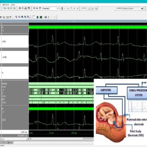
List of the following materials will be included with the Downloaded Backup:Extraction of Fetal ECG from Abdominal and Thorax ECG Using a Non-Causal Adaptive Filter Architecture
Base Paper Abstract:
Extracting the Electrocardiogram (ECG) of a fetus from the ECG signal of the maternal abdomen is a challenging task due to different artifacts. The paper proposes a N-tap non-causal adaptive filter (NC-AF) that update the weight by considering the N number of past weights and N − 1 number of the reference signal and error signal samples after the processing sample number n. Using the maternal abdominal signal as the primary signal and thorax signal as the reference input, the output e(n) is obtained from the mean of N number of errors. The filtering performance of NC-AF was evaluated using the Synthetic dataset and Daisy dataset with the metrics such as correlation coefficient (γ), peak root mean square difference (PRD), the output signal to noise ratio (SNR), root mean square error (RMSE), and fetal R-peak detection accuracy (FRPDA). The NC-AF provides a maximum correlation coefficient, PRD, SNR, RMSE and FRPDA of 0.9851, 83.04%, 8.52 dB, 0.208 and 97.09% respectively with filter length N = 38. The paper also proposes the architecture of NC-AF that can be implemented in hardware like FPGA. Further, the NC-AF was implemented on Virtex-7 FPGA and its performance is evaluated in terms of resource utilization, throughput, and power consumption. For filter length N = 38 and word length L = 24, the maximum performance of the filter can be attained with a power consumption of 1.287W and a maximum clock frequency of 139.47 MHz.
List of the following materials will be included with the Downloaded Backup:Fast and Hardware-Efficient Variable Step Size Adaptive Beamformer
Base Paper Abstract:
Constant step size least mean square (CSS-LMS) is one of the most popular adaptive beamforming algorithms. However, for varying channel signal-to-noise ratios (SNRs), the CSS algorithms are not effective, and there is a need for variable step size (VSS) algorithms. The VSS algorithms provide extremely deep nulls for the interferences; however, they are complex to implement on hardware. Hence, this paper proposes two hardware-efficient variable step size algorithms, namely, efficient variable step size LMS (EVSS-LMS) and reduced complexity parallel LMS (EVSS-RC-pLMS). The proposed EVSS algorithms eliminate the complex operations of VSS algorithms like division and exponential and approximate them to simpler operations. Further, MATLAB simulations demonstrate accelerated convergence, deep nulls, a lower error floor, and better performance in varying SNR environments for the proposed algorithms. Additionally, the finite precision radiation patterns are similar to infinite precision. Hardware synthesis results show the outstanding performance of EVSS in terms of resource utilization on the Xilinx Artix-7 FPGA.
List of the following materials will be included with the Downloaded Backup:FIR Filter Design based on FPGA
Abstract:
FIR (Finite Impulse Response) Filters: the finite impulse response filter is the most basic components in digital signal processing systems are widely used in communications, image processing, and pattern recognition. Based on FPGA(editable logic device) to achieve FIR filter, not only take into account the fixed -function DSP-specific chip real-time, but also has the DSP processor flexibility. The combination of FPGA and DSP technology can further improve integration, increase work speed and expand system capabilities.
List of the following materials will be included with the Downloaded Backup:Floating Point Butterfly Architecture Based on Binary Signed Digit Representation
Fast Fourier transform (FFT) coprocessor, having a significant impact on the performance of communication systems, has been a hot topic of research for many years. The FFT function consists of consecutive multiply add operations over complex numbers, dubbed as butterfly units. Applying floating-point (FP) arithmetic to FFT architectures, specifically butterfly units, has become more popular recently. It offloads compute-intensive tasks from general-purpose processors by dismissing FP concerns (e.g., scaling and overflow/underflow). However, the major downside of FP butterfly is its slowness in comparison with its fixed-point counterpart. This reveals the incentive to develop a high-speed FP butterfly architecture to mitigate FP slowness. This brief proposes a fast FP butterfly unit using a devised FP fused-dot product-add (FDPA) unit, to compute AB±CD±E, based on binary signed-digit (BSD) representation. The FP three-operand BSD adder and the FP BSD constant multiplier are the constituents of the proposed FDPA unit. A carry-limited BSD adder is proposed and used in the three-operand adder and the parallel BSD multiplier so as to improve the speed of the FDPA unit. Moreover, modified Booth encoding is used to accelerate the BSD multiplier. The synthesis results show that the proposed FP butterfly architecture is much faster than previous counterparts but at the cost of more area. The proposed architecture of this paper analysis the logic size, area and power consumption using Xilinx 14.2.
List of the following materials will be included with the Downloaded Backup:FPGA Based High Definition SPWM Generation With Harmonic Mitigation Property
Abstract:
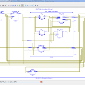
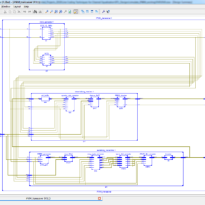
High-resolution sinusoidal pulse width modulation (SPWM) switching is beneficial in order to achieve compact size and fine sinusoidal output of dc–ac converters. In this article, a novel field-programmable gate array (FPGA) based high-definition SPWM (HD-SPWM) architecture is proposed for adopting a scheme of integrating a lower frequency PWM train to a high-frequency SPWM train in order to suppress inverter output harmonics while achieving high resolution output. An optimized FPGA based two-stage finite-state-machine (FSM) architecture is designed, where the initial stage decides pulse widths of a lower frequency PWM train based on the premeditated pulse width of the high-frequency SPWM train, whereas in the final stage, lower frequency PWM pulse widths are integrated with the high-frequency SPWM pulse widths to generate updated pulse widths of high-frequency SPWM, i.e., HD-SPWM. Moreover, a pre-formulation mathematical model is established for the calculation of duty-cycle count values of pulse trains to support the online adjustment of modulation index (MI) of the HD-SPWM. The proposed generation has the benefits of harmonic mitigation, online fine adjustment of MI, low-processing time, and requirement of a minor segment of a medium-sized FPGA; thereby, providing a good tradeoff between larger designs and higher performance. Theoretical calculations, characteristics, and design contemplations are specified, and the HD-SPWM generation is demonstrated through experimentation with a Xilinx Spartan-3 FPGA board.
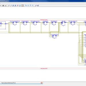
List of the following materials will be included with the Downloaded Backup:FPGA Heart Rate Monitoring (Pre Processing – QRS Detection Stage)
Base Paper Abstract:
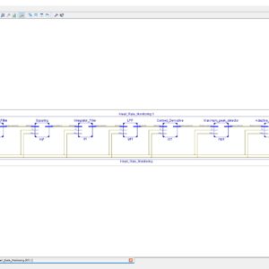
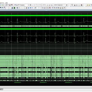
The continuous monitoring of cardiac patients requires an ambulatory system that can automatically detect heart diseases. This study presents a new field programmable gate array (FPGA)-based hardware implementation of the QRS complex detection. The proposed detection system is mainly based on the Pan and Tompkins algorithm, but applying a new, simple, and efficient technique in the detection stage. The new method is based on the centered derivative and the intermediate value theorem, to locate the QRS peaks. The proposed architecture has been implemented on FPGA using the Xilinx System Generator for digital signal processor and the Nexys-4 FPGA evaluation kit. To evaluate the effectiveness of the proposed system, a comparative study has been performed between the resulting performances and those obtained with existing QRS detection systems, in terms of reliability, execution time, and FPGA resources estimation. The proposed architecture has been validated using the 48 half-hours of records obtained from the Massachusetts Institute of Technology - Beth Israel Hospital (MITBIH) arrhythmia database. It has also been validated in real time via the analogue discovery device.
List of the following materials will be included with the Downloaded Backup:FPGA Implementation of a ECG-DAC-SPI Interface for Medical Applications
Proposed Abstract:
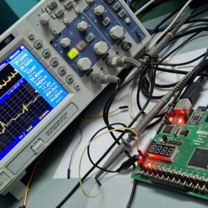
This project presents the design and implementation of an ECG-DAC-SPI interface for medical applications using the Xilinx Spartan-6 FPGA platform and the MCP4921 12-bit SPI DAC. The objective is to process pre-recorded ECG signals from the MIT-BIH database, reconstruct the signal digitally, and output it as an accurate analog waveform suitable for real-time monitoring and simulation. The system is designed to meet the stringent requirements of medical-grade signal fidelity and low-latency processing. The FPGA-based implementation comprises several key modules, including digital ECG data acquisition, optional noise filtering, and a custom SPI communication controller. The ECG signal, preloaded into FPGA memory, is scaled and quantized to match the 12-bit resolution of the MCP4921 DAC. A low-pass FIR filter is implemented on the FPGA to enhance signal quality by removing high-frequency noise, ensuring smooth signal. A Verilog HDL-based SPI controller facilitates precise communication with the DAC, synchronizing data transfer and ensuring real-time signal conversion. The reconstructed analog ECG waveform is visualized on an oscilloscope to validate its fidelity to the original dataset. The DAC, interfaced via the FPGA’s SPI controller, is chosen for its high resolution and compatibility with low-latency applications. The design is synthesized, implemented, and tested on the Xilinx Spartan-6 FPGA platform. The project includes extensive simulation and hardware testing, evaluating parameters such as SPI throughput, waveform accuracy, and system latency. Results demonstrate that the system achieves precise signal reconstruction and reliable analog output, suitable for medical applications. This work highlights the use of FPGA technology and the MCP4921 DAC for scalable and reconfigurable ECG signal processing systems. It provides a robust platform for integration into advanced medical devices, including real-time ECG monitors, simulators, and portable diagnostic tools. Future extensions of the design could include integration of live ECG sensors, advanced noise filtering, or wireless transmission for telemedicine applications.
List of the following materials will be included with the Downloaded Backup:FPGA Implementation of D8PSK Demodulator
Base Paper Abstract:
Differential phase shift keying (DPSK) is a modulation scheme that facilitates non coherent demodulation and is employed for various applications such as Wireless Local Area Networks (WLANs), Bluetooth and RFID communication. In this paper, design, development and hardware implementation of a new demapping scheme for Differential 8-PSK (D8PSK) demodulator on a Zynq 7000 FPGA based ZED board is proposed using the concepts of model based design. The proposed work can be easily extended to other M-ary DPSK schemes.
List of the following materials will be included with the Downloaded Backup:FPGA Implementation of Epileptic Seizure Detection Using ELM Classifier Detection Using ELM Classifier
Abstract:
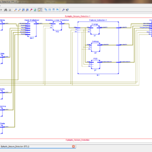
Electroencephalography (EEG) Signals are widely used to determine the brain disorders. The Electrical activity of human brain is recorded in the form of EEG signal. The abnormal Electrical activity of the human brain is called as epileptic seizure. In epilepsy patients, the seizure occurs at unpredictable times and it causes sudden death. Detection and Prediction of Epileptic seizure is performed by analyzing the EEG signal. The EEG signal of human brain is random in nature, hence detection of seizure in EEG signal is challenging task. Hardware implementation of Epileptic seizure detection system is necessary for real time applications. In this work an accurate approach is used to identify the Epileptic seizure and that is implemented in FPGA (Field Programmable Gate Array).The hardware implementation of epileptic seizure detection algorithm is done using Xilinx System generator tool. In the first step the EEG signal is extracted from the human brain and it is filtered by using Finite Impulse response (FIR) band pass filter. The band pass filter separates the EEG signal into delta, theta, alpha, beta and gamma brain rhythms. The band separated brain signal is modeled by linear prediction theory. In the next step features are extracted from the modeled EEG signal and the classification of normal or seizure signal is done by using Extreme Learning Machine (ELM) classifier. The EEG signals used in this paper were obtained from Epilepsy Center at the University of Bonn, Germany. The hardware architecture, Look up tables, resource utilization, Accuracy and power consumption of the algorithm is analyzed using xilinx zynq7000 all programmable soc.
List of the following materials will be included with the Downloaded Backup:FPGA Implementation of Partially Parallel Encoder Architecture for Long Polar Code
Polar coding is an encoding/decoding scheme that provably achieves the capacity of the class of symmetric binary memory-less channels. Due to the channel achieving property, the polar code has become one of the most favourable error-correcting codes. As the polar code achieves the property asymptotically, however, it should be long enough to have a good error-correcting performance. Although previous fully parallel encoder is intuitive and easy to implement, it is not suitable for long polar codes because of the huge hardware complexity required. In the brief, we analyse the encoding process in the viewpoint of very large-scale integration implementation and propose a new efficient encoder architecture that is adequate for long polar codes and effect in alleviating the hardware complexity. As the proposed encoder allows high-throughput encoding with small hardware complexity, it can be systematically applied to the design of any polar code and to any level of parallelism. Finally shown the power, area, delay report with comparison of existing work.
List of the following materials will be included with the Downloaded Backup:
FPGA Implementation of Spread Spectrum Clock Generator with Onion Modulation
Proposed Abstract:
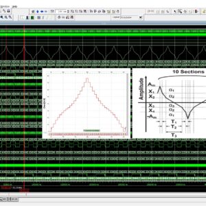
A Spread Spectrum Clock Generator (SSCG) is used in electronics to purposefully vary the frequency of a clock signal via modulation. Modulation is accomplished by dispersing the energy of the signal throughout a spectrum of frequencies rather than focusing it on a certain frequency. The main objective of using the spread spectrum approach in clock generation is to minimize electromagnetic interference (EMI) and enhance electromagnetic compatibility (EMC) in electronic systems. The main reason for using many layers of modulation in spread spectrum clock production, regardless of whether the name "Onion Modulation" is used, is to provide a more advanced and adaptable method for reducing electromagnetic interference. The primary design feature of the onion wave is that the core portion of the waveform has the least steep slope, which serves to generate the output. In order to optimize the frequency effect design, the conventional approach involves using a memory ROM to regulate the slope and obtain the desired onion waveform. This current methodology necessitates substantial memory allocation and an intricate architecture, resulting in higher power consumption. The proposed method presents a unique architecture for onion modulation, which offers reduced logic size and power usage. This architecture was created using Verilog HDL, tested using Modelsim, and implemented using the Xilinx Vertex-5 FPGA.
List of the following materials will be included with the Downloaded Backup:FPGA Implementation of the Adaptive Digital Beamforming for Massive Array
Base Paper Abstract:
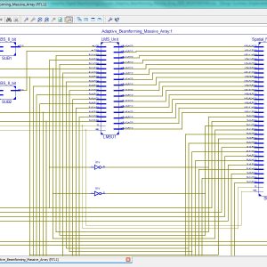
With the rise of 5G networks and the increasing number of communication devices, improving communication quality is essential. One approach is adaptive digital beamforming, which adjusts an antenna array’s radiation pattern based on the desired received signal. Adaptation based on Least-Mean Squared (LMS) and its variants is still one of the most common literature methods. Although LMS techniques present good computational performance, the increase in antennas’ numbers led to high-performance hardware. Platforms such as Field Programmable Gate Arrays (FPGAs), designed for massive array systems, enables high-performance energy-efficient architectures. This work proposes a parallel implementation of a massive array beamforming composed of a spatial filter and adaptation unit based on LMS on FPGA. The proposed design presents ten times fewer hardware requirements and 30 times less power consumption than state of the art.
List of the following materials will be included with the Downloaded Backup:FPGA IP Core for DC Motor Control with Adaptive Neural Network PID Tuning
Base paper Abstract:
Traditional proportional integral derivative (PID) falls short for precise control of DC motor speed under changing conditions. This paper presents a novel FPGA based IP (intellectual property) core for real-time PID parameter adjustment utilizing a multilayer neural network and the back propagation neural network algorithm. The design is implemented entirely in verilog HDL (hardware description language) using the Vivado 2023.1 tool in the Zynq 7z020 SoC (system on chip), with highly efficient resource utilization of 7.37% look-up table (LUT), 1.92% flip-flops, and 3.57% memory. The co-simulation results show a fast rise time of 0.00496s, a settling time of 0.0083s, a lower integral absolute error (IAE) of 0.045, and a minimum overshoot of 0.45%, validating the effectiveness of the proposed controller for comprehensive motion control systems. This dynamic approach outperforms traditional PID controllers by adapting to changing conditions, significantly improving rise time and settling time, which are critical factors in healthcare applications. Other key features of this work include precise duty cycle generation at a 10 kHz switching frequency for accurate motor speed control and an incremental encoder interface for high-resolution position feedback.
List of the following materials will be included with the Downloaded Backup:FPGA-Based System For Heart Rate Monitoring
Abstract:
The continuous monitoring of cardiac patients requires an ambulatory system that can automatically detect heart diseases. This study presents a new field programmable gate array (FPGA)-based hardware implementation of the QRS complex detection. The proposed detection system is mainly based on the Pan and Tompkins algorithm, but applying a new, simple, and efficient technique in the detection stage. The new method is based on the centred derivative and the intermediate value theorem, to locate the QRS peaks. The proposed architecture has been implemented on FPGA using the Xilinx System Generator for digital signal processor and the Nexys-4 FPGA evaluation kit. To evaluate the effectiveness of the proposed system, a comparative study has been performed between the resulting performances and those obtained with existing QRS detection systems, in terms of reliability, execution time, and FPGA resources estimation. The proposed architecture has been validated using the 48 half-hours of records obtained from the Massachusetts Institute of Technology - Beth Israel Hospital (MITBIH) arrhythmia database. It has also been validated in real time via the analogue discovery device.
List of the following materials will be included with the Downloaded Backup:High Performance FIR and IIR Filters Based on FPGA for 16 Hz Signal Processing
Base Paper Abstract:
The goal of the research to design and implement digital filters (Finite Impulse Response (FIR) and Infinite Impulse Response (IIR)) based on Field Programmable Gate Array (FPGA) by using the copulation between MATLAB/Simulink and Xilinx ISE Design Suite programs. low pass digital filter was implemented with different types of windowing methods that calculate the filter coefficient of FIR filter and different types of IIR filter with three numbers of filter order that are (5th order, 8th order, and 10th order). These different types of digital filters and filter orders are applied with the addition of a sine signal with a frequency of 16 Hz and a random noise signal. The work was done by two approaches: the first by simulation method through coupling between MATLAB/Simulink and Xilinx ISE Design Suite programs. While the second is by the practical method of loading these simulation block diagrams on FPGA. The performance of the work is measured by the difference between the sine signal and filtered signal and by the difference between the simulation results and practical results. Using FPGA with digital filters in this research gives a major advantage which is the simulation results equal to the practical results (Difference equal to zero).
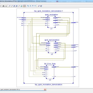
List of the following materials will be included with the Downloaded Backup:High Performance VLSI architecture for M-PSK modems
Abstract:
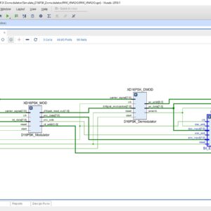
M-PSK (phase shift keying) modulation schemes are used in many high-speed applications like satellite communication, as they are more bandwidth and power efficient compared with other schemes. This study presents very large scale integrated circuits (VLSI) architectures for modulators and demodulators of quadrature phase shift keying (QPSK), 4PSK, 8PSK and 16PSK systems, based on the principle of direct digital synthesis. The proposed modulators do not use any multiplier in contrast to the conventional modulators and hence they are relatively fast and area efficient. Based on the coherent detection technique, this study proposes new demodulation algorithms for 4PSK, 8PSK and 16PSK systems which can be implemented both in analogue and digital domains. This study also presents VLSI architectures for all the proposed algorithms. The proposed architectures are described in VHDL and implemented on Xilinx field programmable gate arrays (FPGAs). The simulation results verify their functional validity and implementation results show the suitability of the proposed architectures for satellite communications.
List of the following materials will be included with the Downloaded Backup:High Speed Low Power and Highly Reliable Frequency Multiplier for DLL Based Clock Generator
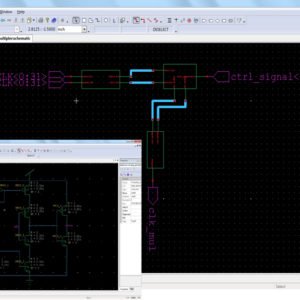
To propose a novel frequency multiplier with high-speed, low-power, and highly reliable design for a delay-locked loop-based clock generator to generate a multiplied clock with a high frequency and wide frequency range. The proposed edge combiner achieves a high-speed and highly reliable operation using a hierarchical structure and an overlap canceller. In addition, by applying the logical effort to the pulse generator and multiplication-ratio control logic design, the proposed frequency multiplier minimizes the delay difference between positive- and negative-edge generation paths, which causes a deterministic jitter. Finally, a numerical analysis is performed to analyze and compare the performance of the proposed frequency multiplier with that of previous frequency multipliers. The proposed frequency multiplier is fabricated using a 0.13-µm CMOS process technology, and has the multiplication ratios of 1, 2, 4, 8, and 16, and an output range of 50 MHz–3.3 GHz. The frequency multiplier achieves power consumption is 17.49mW. The proposed architecture of this paper is analysis the logic size, area and power consumption using tanner tool.
List of the following materials will be included with the Downloaded Backup:
Invasive RLS-Based Fetal ECG Extraction with Optimized Shift-and-Add Multiplier for Area-Efficient FPGA Implementation
Base Paper Abstract:
This article proposes a fetal electrocardiogram (FECG) separation approach based on an energy-dependent recursive least-square (RLS) filtering approach that uses the mother’s R-peaks collected from both the abdomen and the thorax. This approach initially identifies the mother’s R-peaks from the thorax electrocardiogram (ECG), which is used to represent the mother’s R-peaks in both the abdominal and thorax channels. Instead of using the recent abdominal and thorax ECG (TECG) samples, the proposed filter also considers the energy of L1 number of mother’s past R-peak abdominal and thorax samples along with the energy of L2 number of non-R-peak abdominal samples for estimating the R-peak energy factor. The energy factor is estimated for each sample for the updating of weights in the RLS filter. An architecture for the filter is also proposed, which can be used in hardware implementation. The evaluation of the proposed filtering approach was performed using datasets such as Synthetic and Daisy with the evaluation metrics, namely, correlation coefficient, fetal R-peak detection accuracy (PDA), fetal-to-maternal signal-to-noise ratio (SNR), and percent root-mean-square difference. With filter length P = 24, the proposed filter results in correlation, SNR, and percent root-mean-square difference of 0.9901, 9.03 dB, and 80.84%, respectively. For the Daisy and Synthetic datasets, the PDA was estimated as 96.4% and 98.12% respectively. The architecture of the proposed filter was implemented in Virtex VC707 hardware, which utilizes a power of 1.378 W, resulting in a maximum clock frequency and throughput (TP) of 128.43 MHz and 31.5 Mb/s, respectively, with a word length of L = 24 bits.
List of the following materials will be included with the Downloaded Backup:Line Coding Techniques for Channel Equalization: Integrated Pulse-Width Modulation and Consecutive Digit Chopping
Abstract:
This paper presents two new line-coding schemes, integrated pulse width modulation (iPWM) and consecutive digit chopping (CDC) for equalizing lossy wire line channels with the aim of achieving energy efficient wire line communication. The proposed technology friendly encoding schemes are able to overcome the fundamental limitations imposed by Manchester or pulse-width modulation encoding on high-speed wire line transceivers. A highly digital encoder architecture is leveraged to implement the proposed iPWM and CDC encoding. Energy-efficient operation of the proposed encoding is demonstrated on a high-speed wire line transceiver that can operate from 10 to 18 Gb/s. Fabricated in a 65-nm CMOS process, the transceiver operates with supply voltages of 0.9 V, 1 V, and 1.1 V. With the help of the proposed iPWM encoding, the transceiver can equalize over 27-dB of channel loss while operating at 16 Gb/s with an efficiency of 4.37 pJ/bit. The design occupies an active die area of 0.21 mm2.
List of the following materials will be included with the Downloaded Backup:Low Power Compressor Based MAC Architecture for DSP Applications
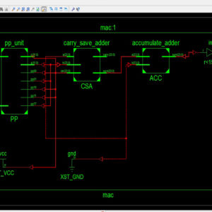
This paper presents the low power compressor based Multiply-Accumulate (MAC) architecture for DSP applications. In VLSI, highly computed arithmetic cells including adders and multipliers are the most copiously used components. Efficient implementation of arithmetic logic units, floating point units and other dedicated functional components are utilized in most of the microprocessors and digital signal processors (DSPs). Thus in this brief, compressor circuit has been illustrated for the low power applications and also the impact of datapath circuits has been demonstrated. The proposed low power compressor architecture was applied to MAC unit and compared against the conventional compressor based MAC units and observed that the proposed architecture has reduced significant amount of leakage power. The proposed architecture of this paper analysis the logic size, area and power consumption using Xilinx 14.2.
List of the following materials will be included with the Downloaded Backup:
Low Power Split Radix FFT Processors Using Radix 2 Butterfly Units
Split radix fast Fourier Transform (SRFFT) is an ideal candidate for the implementation of a low power FFT processor, because it has the lowest number of arithmetic operation among all the FFT algorithms. In the design of such processors, an efficient addressing scheme for FFT data as well as twiddle factors is required. The signal flow graph of SRFFT is the same as radix-2 FFT, and therefore, the conventional address generation schemes of FFT data could also be applied to SRFFT. However SRFFT has irregular locations of twiddle factors and forbids the application of radix-2 address generation methods. This brief presents a shared memory low power SRFFT processor architecture. The SRFFT can be computed by using a modified radix-2 butterfly unit. The butterfly unit exploits the multiplier-gating technique to save dynamic power at the expense of using more hardware resources. In addition, two novel address generation algorithm for both the trivial and nontrivial twiddle factors are developed. In this paper We increases the architecture size, of radix-4 and 2048 point complex valued transform, and shown the performance of area, power and delay, and synthesized xilinx FPGA on s6lx16-2csg225.
List of the following materials will be included with the Downloaded Backup:Low Power System for Detection of Symptomatic Patterns in Audio Biological Signals
We present a low-power, efficacious, and scalable system for the detection of symptomatic patterns in biological audio signals. The digital audio recordings of various symptoms, such as cough, sneeze, and so on, are spectrally analyzed using a discrete wavelet transform. Subsequently, we use simple mathematical metrics, such as energy, quasi-average, and coastline parameter for various wavelet coefficients of interest depending on the type of pattern to be detected. Furthermore, a mel-frequency cepstrum-based analysis is applied to distinguish between signals, such as cough and sneeze, which have a similar frequency response and, hence, occur in common wavelet coefficients. Algorithm-circuit codesign methodology is utilized in order to optimize the system at algorithm and circuit levels of design abstraction. This helps in implementing a low-power system as well as maintaining the efficacy of detection. The system is scalable in terms of user specificity as well as the type of signal to be analyzed for an audio symptomatic pattern. The proposed architecture of this paper analysis the logic size, area and power consumption using Xilinx 14.2.
List of the following materials will be included with the Downloaded Backup:Low-Complexity 2-D Digital FIR Filters Using Polyphase Decomposition and Farrow Structure
Abstract:
This paper proposes a novel realization technique for quadrantally symmetric 2-D finite impulse response filters with a guaranteed reduction in the hardware complexity. Here, the concept of Farrow structure-based interpolation filter design using the polyphase decomposition of the 1-D filter transfer function is effectively utilized in the 2-D domain. The proposed 2-D filter makes use of row-wise polyphase decomposition of the 2-D transfer function or frequency response, followed by the polynomial approximation of the individual polyphase coefficients resulting in Farrow structures corresponding to each row filter. The final coefficients are implemented by varying the delay values in all the Farrow structures, followed by the interpolation of the coefficients obtained from each delay value, which in turn forms the rows in the 2-D kernel. The major highlight of the proposed method is the highly reduced implementation complexity in terms of the number of multipliers and adders, with a low normalized root-mean-square error. Design examples of the circularly symmetric and fan-type filters have been considered to show the efficiency of the approach. The results show a drastic reduction in the implementation complexity of the 2-D filters of upto 20%, with significantly low normalized root-mean-square error lesser than 0.5%.
List of the following materials will be included with the Downloaded Backup:Low-Complexity Implementation of Real-Time Reconfigurable Low-Pass Equalizers
Implementation techniques and results for a recently proposed real-time reconfigurable low-pass equalizer (RLPE) consisting of a variable bandwidth (VBW) filter and a variable equalizer (VE) are presented. Both components utilize fixed finite-length impulse response (FIR) filters combined with a few general multipliers, resulting in lower area and power consumption compared to a general FIR filter, despite requiring more multiplications. This is because the constant multipliers in the fixed FIR filters of the RLPE can be optimized for implementation. An additional advantage is that the proposed RLPE does not require online design. Various implementation alternatives for fixed FIR filters, including ways to increase the frequency, are evaluated to optimize the implementation of the RLPE. Several versions of the proposed RLPE and a general FIR filter for comparison are implemented using a 28-nm fully depleted silicon on insulator (FD-SOI) standard cell library. The results demonstrate that the RLPE baseline design requires less power and area than the general equalizer, and although the frequency of the baseline implementation is lower, the design can reach the same frequency while still having significantly less power and area. Furthermore, an approach is introduced to break the chain in the polynomial section of the VBW filter by using fewer additional registers compared to standard pipelining. Instead, this method reformulates the constant multiplication problem to produce correct results. For the considered case, the power consumption is reduced between 49% and 70% for different frequencies, with an area decrease in the range of 64% to 67%, by using the proposed RLPE compared to a general FIR filter. Index Terms: Constant multiplications, real-time reconfiguration, variable bandwidth (VBW) low-pass filter, variable equalizer (VE).
List of the following materials will be included with the Downloaded Backup:Low-Complexity VLSI Design of Large Integer Multipliers for Fully Homomorphic Encryption
Abstract:
Large integer multiplication has been widely used in fully homomorphic encryption (FHE). Implementing feasible large integer multiplication hardware is thus critical for accelerating the FHE evaluation process. In this paper, a novel and efficient operand reduction scheme is proposed to reduce the area requirement of radix-r butterfly units. We also extend the single port, merged-bank memory structure to the design of number theoretic transform (NTT) and inverse NTT (INTT) for further area minimization. In addition, an efficient memory addressing scheme is developed to support both NTT/INTT and resolving carries computations. Experimental results reveal that significant area reductions can be achieved for the targeted 786 432- and 1 179 648-bit NTT-based multipliers designed using the proposed schemes in comparison with the related works. Moreover, the two multiplications can be accomplished in 0.196 and 2.21 ms, respectively, based on 90-nm CMOS technology. The low-complexity feature of the proposed large integer multiplier designs is thus obtained without sacrificing the time performance.
List of the following materials will be included with the Downloaded Backup:Low-Cost High-Performance VLSI Architecture for Montgomery Modular Multiplication
Source Code : VHDL & VERILOG HDL
Abstract: This paper proposes a simple and efficient Montgomery multiplication algorithm such that the low-costand high-performance Montgomery modular multiplier can be implemented accordingly. The proposed multiplier output data with representation and uses only one parallel prefix adder to avoid a carry propagation and reduce the area, power and delay, and also increasing the speed. Mainly the usage of parallel prefix adder is to reduce the significant delay reduction and area × time2 improvements, all this at the cost of higher power consumption, which is the main reason preventing the use of parallel-prefix adders to achieve high-speed reverse converters in nowadays systems. Hence, to solve the high power consumption problem, novel specific hybrid parallel-prefix-based adder components those provide better trade-off between delay and power consumption. As a result, the extra clock cycles for operand pre-computation and format conversion can be hidden and high throughput can be obtained. Experimental results show that the proposed Montgomery modular multiplier can achieve higher performance and significant area–time product improvement when compared with previous designs. Using VHDL to design the RTL, and the result to be shown in Xilinx 14.2 with Power consumption and area reduction.
List of the following materials will be included with the Downloaded Backup:
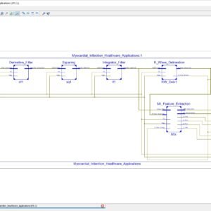
MInSC: A VLSI Architecture for Myocardial Infarction Stages Classifier for Wearable Healthcare Applications
Base Paper Abstract:
Myocardial Infarction (MI) is a critical heart abnormality causing millions of fatalities worldwide every year. MI progress in three stages based on its severity causing several changes in an Electrocardiogram (ECG) signal. It is very critical to capture these variations, which requires continuous monitoring of the ECG signal of the patient. Therefore, it becomes imperative to develop a low power VLSI architecture to address the prognosis of MI. In this brief, for the first time, an area and power efficient design of a five stage classifier is proposed, which detects the progression of various stages of MI using ECG beats in real time. The proposed architecture has an area and total power utilization of 1.38mm2 and 5.12µW, respectively at SCL 180nm Bulk CMOS technology. The low power and area requirements and multiclass classification capability of the proposed design make it suitable to be used in wearable devices.
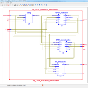
List of the following materials will be included with the Downloaded Backup:QPSK Modulator on FPGA
Abstract:
The paper presents the theoretical backgrounds of a QPSK Modulation. The QPSK Modulator is then simulated using Modelsim and Xilinx environment tool for FPGA design as well as implemented on a Spartan 6 LX9 FPGA. The modulator algorithm has been implemented on FPGA using the Verilg HDL language on Xilinx ISE 14.2. The local clock oscillator of the board is 50Mhz which corresponds with a period of 20ns. The frequency of the QPSK carrier is 31,250 kHz and because the QPSK symbol is made of two bits, the output frequency is 62,50kbps. The modulator has been designed and simulated and its performances were evaluated by measurements.
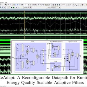
List of the following materials will be included with the Downloaded Backup:ReAdapt: A Reconfigurable Datapath for Runtime Energy-Quality Scalable Adaptive Filters
Base Paper Abstract:
This paper proposes ReAdapt–a reconfigurable datapath architecture for scaling the energy-quality trade-off of adaptive filtering at runtime. The ReAdapt can dynamically select four adaptive filtering algorithms for gradating complexity levels during runtime by reconfiguring the processing flow in its datapath and by blocking the switching activity (e.g., reducing the CMOS dynamic power) of unused modules with data-gating. The ReAdapt proposal can scale the energy-quality trade-off by choosing the following four different levels of filter algorithms complexity: 1) least mean square (LMS); 2) partial update normalized LMS (PU-NLMS); 3) set-membership normalized LMS (SM-NLMS); 4) normalized LMS (NLMS). The ReAdapt architecture reuses common modules of each adaptive filter, resulting in a compact VLSI hardware implementation. The ReAdapt architecture operation is implemented in a case-study for interference mitigation for electroencephalogram (EEG) signal processing. The hardware synthesis results show an increase of 6.80 times in throughput and at least a reduction of 2.84 times in energy per operation compared with the state-of-the-art adaptive filters. This paper also investigates the benefits of dynamically reconfiguring the four ReAdapt operating modes at runtime for different levels of signal-to-noise ratio (SNR) for the processed signals. We also demonstrate that dynamically reconfiguring the ReAdapt operating modes during runtime results in an optimal energy-quality trade-off which is advantageous over the conventional single static mode.
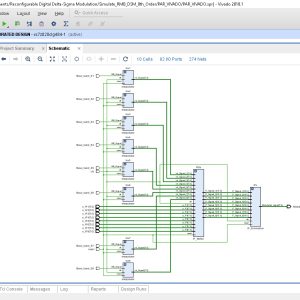
List of the following materials will be included with the Downloaded Backup:Reconfigurable Digital Delta-Sigma Modulation Transmitter Architecture for Concurrent Multi-Band Transmission
Abstract:
This paper presents a reconfigurable delta-sigma modulation (DSM) architecture for concurrent multi-band transmission. The reconfigurability in terms of carrier spacing and the number of simultaneous carrier transmission is useful for applications such as carrier aggregation in 5G. This paper uses 4th order reconfigurable multi-band DSM (RMB-DSM) such that the zeros of the noise transfer function can be reconfigured to fall at multiple frequencies, where the carriers are being aggregated. The quantization noise between the transmission bands is a critical issue in the case of multi-band transmission. Therefore, a multi-band additional noise shaping (ANS) function is also introduced, which generates notches around each carrier and reduces the noise level between the multiple pass-bands. The proposed scheme has been validated in simulation, as well as in experiment for aggregating up to four 15 MHz long term evolution (LTE) signals with an overall aggregated bandwidth of 60 MHz. Measurement results show a 10-25% improvement in coding efficiency and 15-35 dB improvement in noise level near the operating frequency band using the proposed multiband augmented noise shaping technique, as compared to the standard DSM. The corresponding improvement of 8% in the overall efficiency is observed by using the proposed multi-band augmented noise shaping technique.
List of the following materials will be included with the Downloaded Backup:RF Power Gating A Low Power Technique for Adaptive Radios
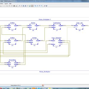
RoBA Multiplier A Rounding Based Approximate Multiplier for High Speed yet Energy Efficient Digital Signal Processing
Abstract:
In this paper, we propose an approximate multiplier that is high speed yet energy efficient. The approach is to round the operands to the nearest exponent of two. This way the computational intensive part of the multiplication is omitted improving speed and energy consumption at the price of a small error. The proposed approach is applicable to both signed and unsigned multiplications. We propose three hardware implementations of the approximate multiplier that includes one for the unsigned and two for the signed operations. The efficiency of the proposed multiplier is evaluated by comparing its performance with those of some approximate and accurate multipliers using different design parameters. In addition, the efficacy of the proposed approximate multiplier is studied in two image processing applications, i.e., image sharpening and smoothing.
List of the following materials will be included with the Downloaded Backup:Sparse FIR Filter Design via Partial 1-Norm Optimization
Abstract:
Electrocardiogram (ECG) is a form of cardiovascular measurement, for the diagnosis of different heart rate conditions. However, numerous noises usually harm the amplitude and time period of the signal from the ECG signal, at following a transition of the analog ECG signal from the sensor module into a digital format. The appropriate digital filter may be used to remove different forms of noise such as Baseline Wander, Power line interference, High frequency noise and Physiological Artifacts. The Digital FIR filter will have prospected to reduced the artifacts in the ECG signals. The signals taken from the MIT-BIH data base which contains the normal and abnormal waveforms. This Digital FIR filter can have more performance by using more TAP numbers such as multiplying, delaying and getting more effectiveness. This proposed work would implement a 1 norm minimization in the FIR filter with liner step method to minimize sparse complexity and reduce the mini-max approximation error for sparse maximization. Given these facts, several rules for selecting indicators of potential zero coefficients to be used in 1 standard optimization are adopted in the proposed algorithm. The efficacy of the proposed design algorithm was developed in Verilog HDL, simulated in Modelsim software and synthesized in Xilinx vertex 5 FPGA, and finally prove all the parameters in terms of area, delay and power.
List of the following materials will be included with the Downloaded Backup:To develop and Implement Low Power, High Speed VLSI for Processing Signals using Multi rate Techniques Low Power Divider Using Vedic Mathematics
Abstract:
Multirate technique is necessary for systems with different input and output sampling rates. Recent advances in mobile computing and communication applications demand low power and high speed VLSI DSP systems. In this paper to discuss the downsampling technique and its improvement, major drawbacks of present approaches possible to increase degeneracy. This Multirate design methodology is systematic and applicable to many problems. The proposed architecture of this paper analysis the logic size, area and power consumption using Xilinx 14.2.The proposed architecture of this paper analysis the logic size, area and power consumption using Xilinx 14.2.
List of the following materials will be included with the Downloaded Backup:VLSI Design of SVM-Based Seizure Detection System With On-Chip Learning Capability
Abstract:
Portable automatic seizure detection system is very convenient for epilepsy patients to carry. In order to make the system on-chip trainable with high efficiency and attain high detection accuracy, this paper presents a very large scale integration (VLSI) design based on the nonlinear support vector machine (SVM). The proposed design mainly consists of a feature extraction (FE) module and an SVM module. The FE module performs the three level Daubechies discrete wavelet transform to fit the physiological bands of the electroencephalogram (EEG) signal and extracts the time–frequency domain features reflecting the non stationary signal properties. The SVM module integrates the modified sequential minimal optimization algorithm with the table-driven-based Gaussian kernel to enable efficient on-chip learning. The presented design is verified on an Altera Cyclone II field-programmable gate array and tested using the two publicly available EEG datasets. Experiment results show that the designed VLSI system improves the detection accuracy and training efficiency.
List of the following materials will be included with the Downloaded Backup:World’s Fastest FFT Architectures: Breaking the Barrier of 100 GS/s
Abstract:
This paper presents the fastest fast Fourier transform (FFT) hardware architectures so far. The architectures are based on a fully parallel implementation of the FFT algorithm. In order to obtain the highest throughput while keeping the resource utilization low, we base our design on making use of advanced shift-and-add techniques to implement the rotators and on selecting the most suitable FFT algorithms for these architectures. Apart from high throughput and resource efficiency, we also guarantee high accuracy in the proposed architectures. For the implementation, we have developed an automatic tool that generates the architectures as a function of the FFT size, input word length and accuracy of the rotations. We provide experimental results covering various FFT sizes, FFT algorithms, and field-programmable gate array boards. These results show that it is possible to break the barrier of 100 GS/s for FFT calculation.
List of the following materials will be included with the Downloaded Backup:Provide Wordlwide Online Support
We can provide Online Support Wordlwide, with proper execution, explanation and additionally provide explanation video file for execution and explanations.
24/7 Support Center
NXFEE, will Provide on 24x7 Online Support, You can call or text at +91 9789443203, or email us nxfee.innovation@gmail.com
Terms & Conditions:
Customer are advice to watch the project video file output, and before the payment to test the requirement, correction will be applicable.
After payment, if any correction in the Project is accepted, but requirement changes is applicable with updated charges based upon the requirement.
After payment the student having doubts, correction, software error, hardware errors, coding doubts are accepted.
Online support will not be given more than 3 times.
On first time explanation we can provide completely with video file support, other 2 we can provide doubt clarifications only.
If any Issue on Software license / System Error we can support and rectify that within end of day.
Extra Charges For duplicate bill copy. Bill must be paid in full, No part payment will be accepted.
After payment, to must send the payment receipt to our email id.
Powered by NXFEE INNOVATION, Pondicherry.
Call us today at : +91 9789443203 or Email us at nxfee.innovation@gmail.com
NXFEE Development & Services

Product Categories
- 2014 (11)
- 2015 (39)
- 2016 (30)
- 2017 (16)
- 2018 (17)
- 2019 (42)
- 2020 (29)
- 2021 (17)
- 2022 (23)
- Accessories (45)
- Area Efficient (117)
- High speed VLSI Design (56)
- IEEE (15)
- Image Processing (40)
- Low power VLSI Design (98)
- NOC VLSI Design (2)
- VLSI (251)
- VLSI 2023 (21)
- VLSI 2024 (18)
- VLSI 2025 (31)
- VLSI 2026 (4)
- VLSI Application / Interface and Mini Projects (31)
- VLSI_2023 (15)
Filter by price
Product Status
Sort by producents

Copyright © 2026 Nxfee Innovation.

